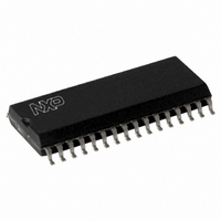
MFRC53001T/0FE,112 NXP Semiconductors, MFRC53001T/0FE,112 Datasheet - Page 9

MFRC53001T/0FE,112
Manufacturer Part Number
MFRC53001T/0FE,112
Description
IC MIFARE HS READER 32-SOIC
Manufacturer
NXP Semiconductors
Series
MIFARE®r
Specifications of MFRC53001T/0FE,112
Rf Type
Read Only
Frequency
13.56MHz
Features
ISO14443-A, ISO14443-B, ISO15693
Package / Case
32-SOIC (0.300", 7.50mm Width)
Product
RFID Readers
Operating Temperature Range
- 25 C to + 85 C
Lead Free Status / RoHS Status
Lead free / RoHS Compliant
Lead Free Status / RoHS Status
Lead free / RoHS Compliant, Lead free / RoHS Compliant
Other names
568-2223-5
935269692112
MFRC530
MFRC53T0FED
935269692112
MFRC530
MFRC53T0FED
Available stocks
Company
Part Number
Manufacturer
Quantity
Price
Company:
Part Number:
MFRC53001T/0FE,112
Manufacturer:
MICROCHIP
Quantity:
12 000
NXP Semiconductors
MFRC530_33
Product data sheet
PUBLIC
Fig 4.
Connection to microprocessor: common read and write strobes
address bus (A3 to An)
address bus (A0 to A2)
data bus (D0 to D7)
HIGH
Data strobe (NDS)
Read/Write (R/NW)
9.1.3.2 Common read and write strobe
9.1.3.3 Common read and write strobe: EPP with handshake
9.1.4 Serial Peripheral Interface
Refer to
Refer to
Remark: In the EPP standard a chip select signal is not defined. To cover this situation,
the status of the NCS pin can be used to inhibit the nDStrb signal. If this inhibitor is not
used, it is mandatory that pin NCS is connected to pin DVSS.
Remark: After each Power-On or Hard reset, the nWait signal on pin A0 is
high-impedance. nWait is defined as the first negative edge applied to the nAStrb pin after
the reset phase. The MFRC530 does not support Read Address Cycle.
The MFRC530 provides compatibility with the 5-wire Serial Peripheral Interface (SPI)
standard and acts as a slave during the SPI communication. The SPI clock signal SCK
must be generated by the master. Data communication from the master to the slave uses
the MOSI line. The MISO line sends data from the MFRC530 to the master.
Fig 5.
DECODER
ADDRESS
Section 13.4.2 on page 92
Section 13.4.3 on page 93
Connection to microprocessor: EPP common read/write strobes and handshake
All information provided in this document is subject to legal disclaimers.
NCS
A0 to A2
D0 to D7
ALE
NRD
NWR
DEVICE
Rev. 3.3 — 6 July 2010
multiplexed address/data (AD0 to AD7)
Address strobe (nAStrb)
Data strobe (nDStrb)
Read/Write (nWrite)
LOW
HIGH
HIGH
nWait
057433
for timing specification.
for timing specification.
non-multiplexed address
LOW
HIGH
LOW
multiplexed address/data (AD0 to AD7)
Address strobe (AS)
Data strobe (NDS)
Read/Write (R/NW)
NCS
A2
A1
A0
AD0 to AD7
ALE
NRD
NWR
DECODER
ADDRESS
DEVICE
001aak609
ISO/IEC 14443 A Reader IC
NCS
A2
A1
A0
AD0 to AD7
ALE
NRD
NWR
MFRC530
DEVICE
© NXP B.V. 2010. All rights reserved.
001aak608
9 of 115


