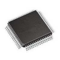
PIC18F65K90T-I/PT Microchip Technology, PIC18F65K90T-I/PT Datasheet - Page 157

PIC18F65K90T-I/PT
Manufacturer Part Number
PIC18F65K90T-I/PT
Description
32kB Flash, 2kB RAM, 1kB EE, NanoWatt XLP, LCD 64 TQFP 10x10x1mm T/R
Manufacturer
Microchip Technology
Series
PIC® XLP™ 18Fr
Datasheet
1.PIC18F66K90-IMR.pdf
(570 pages)
Specifications of PIC18F65K90T-I/PT
Processor Series
PIC18F
Core
PIC
Data Bus Width
8 bit
Program Memory Type
Flash
Program Memory Size
32 KB
Data Ram Size
2 KB
Interface Type
I2C, SPI
Maximum Clock Frequency
64 MHz
Number Of Timers
8
Operating Supply Voltage
1.8 V to 5.5 V
Maximum Operating Temperature
+ 125 C
3rd Party Development Tools
52715-96, 52716-328, 52717-734, 52712-325, EWPIC18
Minimum Operating Temperature
- 40 C
On-chip Adc
12 bit, 16 Channel
Core Processor
PIC
Core Size
8-Bit
Speed
64MHz
Connectivity
I²C, LIN, SPI, UART/USART
Peripherals
Brown-out Detect/Reset, LCD, POR, PWM, WDT
Number Of I /o
53
Eeprom Size
1K x 8
Ram Size
2K x 8
Voltage - Supply (vcc/vdd)
1.8 V ~ 5.5 V
Data Converters
A/D 16x12b
Oscillator Type
Internal
Operating Temperature
-40°C ~ 85°C
Package / Case
64-TQFP
Lead Free Status / Rohs Status
Details
Available stocks
Company
Part Number
Manufacturer
Quantity
Price
Company:
Part Number:
PIC18F65K90T-I/PT
Manufacturer:
Microchip Technology
Quantity:
10 000
Company:
Part Number:
PIC18F65K90T-I/PTRSL
Manufacturer:
Microchip Technology
Quantity:
10 000
- Current page: 157 of 570
- Download datasheet (5Mb)
11.2
PORTA is an 8-bit wide, bidirectional port. The corre-
sponding Data Direction and Output Latch registers are
TRISA and LATA.
RA4/T0CKI is a Schmitt Trigger input. All other PORTA
pins have TTL input levels and full CMOS output
drivers.
The RA4 pin is multiplexed with the Timer0 clock input
and one of the LCD segment drives. RA5 and RA<3:0>
are multiplexed with analog inputs for the A/D
Converter. RA1 is multiplexed with analog as well as
the LCD segment drive.
The operation of the analog inputs as A/D Converter
inputs is selected by clearing or setting the
ANSEL<3:0> control bits in the ANCON1 register. The
corresponding TRISA bits control the direction of these
pins, even when they are being used as analog inputs.
The user must ensure the bits in the TRISA register are
maintained set when using them as analog inputs.
2009-2011 Microchip Technology Inc.
Note:
PORTA, TRISA and
LATA Registers
RA5 and RA<3:0> are configured as
analog inputs on any Reset and are read
as ‘0’. RA4 is configured as a digital input.
PIC18F87K90 FAMILY
OSC2/CLKO/RA6
serve as the external circuit connections for the exter-
nal (primary) oscillator circuit (HS Oscillator modes) or
the external clock input and output (EC Oscillator
modes). In these cases, RA6 and RA7 are not available
as digital I/O and their corresponding TRIS and LAT
bits are read as ‘0’. When the device is configured to
use HF-INTOSC, MF-INTOSC or LF-INTOSC as the
default oscillator mode, RA6 and RA7 are automatically
configured as digital I/O; the oscillator and clock
in/clock out functions are disabled.
RA1, RA4 and RA5 are multiplexed with LCD segment
drives that are controlled by bits in the LCDSE1 and
LCDSE2 registers. I/O port functionality is only
available when the LCD segments are disabled.
RA5 has additional functionality for Timer1 and Timer3.
It can be configured as the Timer1 clock input or the
Timer3 external clock gate input.
EXAMPLE 11-1:
CLRF
CLRF
BANKSEL ANCON1
MOVLW
MOVWF
MOVLW
MOVWF
PORTA
LATA
00h
ANCON1 ; for digital inputs
0BFh
TRISA
and
; Initialize PORTA by
; clearing output latches
; Alternate method to
; clear output data latches
; Configure A/D
; Value used to initialize
; data direction
; Set RA<7, 5:0> as inputs,
; RA<6> as output
INITIALIZING PORTA
OSC1/CLKI/RA7
DS39957D-page 157
normally
Related parts for PIC18F65K90T-I/PT
Image
Part Number
Description
Manufacturer
Datasheet
Request
R

Part Number:
Description:
Manufacturer:
Microchip Technology Inc.
Datasheet:

Part Number:
Description:
Manufacturer:
Microchip Technology Inc.
Datasheet:

Part Number:
Description:
Manufacturer:
Microchip Technology Inc.
Datasheet:

Part Number:
Description:
Manufacturer:
Microchip Technology Inc.
Datasheet:

Part Number:
Description:
Manufacturer:
Microchip Technology Inc.
Datasheet:

Part Number:
Description:
Manufacturer:
Microchip Technology Inc.
Datasheet:

Part Number:
Description:
Manufacturer:
Microchip Technology Inc.
Datasheet:

Part Number:
Description:
Manufacturer:
Microchip Technology Inc.
Datasheet:


