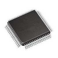
PIC18F65K90T-I/PT Microchip Technology, PIC18F65K90T-I/PT Datasheet - Page 95

PIC18F65K90T-I/PT
Manufacturer Part Number
PIC18F65K90T-I/PT
Description
32kB Flash, 2kB RAM, 1kB EE, NanoWatt XLP, LCD 64 TQFP 10x10x1mm T/R
Manufacturer
Microchip Technology
Series
PIC® XLP™ 18Fr
Datasheet
1.PIC18F66K90-IMR.pdf
(570 pages)
Specifications of PIC18F65K90T-I/PT
Processor Series
PIC18F
Core
PIC
Data Bus Width
8 bit
Program Memory Type
Flash
Program Memory Size
32 KB
Data Ram Size
2 KB
Interface Type
I2C, SPI
Maximum Clock Frequency
64 MHz
Number Of Timers
8
Operating Supply Voltage
1.8 V to 5.5 V
Maximum Operating Temperature
+ 125 C
3rd Party Development Tools
52715-96, 52716-328, 52717-734, 52712-325, EWPIC18
Minimum Operating Temperature
- 40 C
On-chip Adc
12 bit, 16 Channel
Core Processor
PIC
Core Size
8-Bit
Speed
64MHz
Connectivity
I²C, LIN, SPI, UART/USART
Peripherals
Brown-out Detect/Reset, LCD, POR, PWM, WDT
Number Of I /o
53
Eeprom Size
1K x 8
Ram Size
2K x 8
Voltage - Supply (vcc/vdd)
1.8 V ~ 5.5 V
Data Converters
A/D 16x12b
Oscillator Type
Internal
Operating Temperature
-40°C ~ 85°C
Package / Case
64-TQFP
Lead Free Status / Rohs Status
Details
Available stocks
Company
Part Number
Manufacturer
Quantity
Price
Company:
Part Number:
PIC18F65K90T-I/PT
Manufacturer:
Microchip Technology
Quantity:
10 000
Company:
Part Number:
PIC18F65K90T-I/PTRSL
Manufacturer:
Microchip Technology
Quantity:
10 000
- Current page: 95 of 570
- Download datasheet (5Mb)
6.3.4
The Special Function Registers (SFRs) are registers
used by the CPU and peripheral modules for controlling
the desired operation of the device. These registers are
implemented as static RAM. SFRs start at the top of
data memory (FFFh) and extend downward to occupy
all of Bank 15 (F00h to FFFh) and the top part of
Bank 14 (EF4h to EFFh).
A list of these registers is given in
Table
TABLE 6-1:
2009-2011 Microchip Technology Inc.
Note 1:
FEDh POSTDEC0
FECh PREINC0
Addr.
FFDh
FFCh
FEEh POSTINC0
FEBh PLUSW0
FEAh
FFEh
FFBh
FEFh
FFFh
FFAh
FF9h
FF8h
FF7h
FF6h
FF5h
FF4h
FF3h
FF2h
FF1h
FF0h
FE9h
FE8h
FE7h
FE6h POSTINC1
FE5h POSTDEC1
FE4h PREINC1
FE3h PLUSW1
FE2h
FE1h
FE0h
F3Fh
6-2.
2:
3:
4:
5:
TBLPTRU
TBLPTRH
TBLPTRL
INTCON2
INTCON3
TMR7H
STKPTR
PCLATU
PCLATH
INTCON
INDF0
INDF1
TABLAT
PRODH
PRODL
FSR0H
FSR1H
FSR0L
WREG
FSR1L
Name
TOSU
TOSH
TOSL
PCL
BSR
This is not a physical register.
Unimplemented registers are read as ‘0’.
This register is not available in 64-pin devices (PIC18F6XK90).
This register is not available in devices with a program memory of 32 Kbytes (PIC18FX5K90).
Addresses, EF4h through F5Fh, are also used by SFRs, but are not part of the Access RAM. Users must always load
the proper BSR value to access these registers.
SPECIAL FUNCTION REGISTERS
(1)
(1)
(4)
(1)
(1)
(1)
(1)
(1)
(1)
(1)
(1)
PIC18F87K90 FAMILY SPECIAL FUNCTION REGISTER MAP
FDDh POSTDEC2
FDCh PREINC2
FCDh
FCCh
Addr.
FDEh POSTINC2
FDBh PLUSW2
FDAh
FCEh
FCBh
FCAh
FDFh
FD9h
FD8h
FD7h
FD6h
FD5h
FD4h SPBRGH1
FD3h
FD2h
FD1h
FD0h
FCFh
FC9h
FC8h
FC7h SSP1STAT
FC6h SSP1CON1
FC5h SSP1CON2
FC4h
FC3h
FC2h
FC1h
FC0h
F32h
SSP1BUF
SSP1ADD
WDTCON
OSCCON
TMR12
ADRESH
ADCON0
ADCON1
ADCON2
ADRESL
INDF2
STATUS
TMR0H
T0CON
TMR1H
T1CON
T2CON
FSR2H
TMR0L
TMR1L
FSR2L
RCON
Name
TMR2
IPR5
PR2
(1)
(4)
(1)
(1)
(1)
(1)
Table 6-1
Addr.
FBDh
FBCh
FBFh ECCP1AS
FBEh ECCP1DEL
FBBh CCP1CON
FBAh
FAEh
FADh
FACh
FABh
FAAh
FB9h
FB8h
FB7h
FB6h
FB5h
FB4h
FB3h
FB2h
FB1h
FB0h
FAFh
FA9h
FA8h HLVDCON
FA7h
FA6h
FA5h
FA4h
FA3h
FA2h
FA1h
FA0h
F25h
CVRCON
T3GCON
RCREG1
T1GCON
ANCON0
CCPR1H
SPBRG1
CCPR1L
CMSTAT
TXREG1
RCSTA1
TXSTA1
TMR3H
TMR3L
T3CON
Name
PIR5
IPR4
PIR4
IPR6
PIR6
IPR3
PIR3
IPR2
PIR2
PIE5
PIE4
PIE3
PIE2
—
and
(2)
Addr.
F9Dh
F9Ch PSTR1CON F7Ch LCDDATA22
F8Dh
F8Ch
F9Eh
F9Bh OSCTUNE F7Bh
F9Ah
F8Eh
F8Bh
F8Ah
F9Fh
F99h TRISH
F98h
F97h
F96h
F94h
F93h
F92h
F91h
F90h
F8Fh
F89h
F88h PORTJ
F87h PORTH
F86h
F85h
F84h
F83h
F82h
F81h
F80h
F18h
F95h
PIC18F87K90 FAMILY
The SFRs can be classified into two sets: those
associated with the “core” device functionality (ALU,
Resets and interrupts) and those related to the
peripheral functions. The Reset and Interrupt registers
are described in their respective chapters, while the
ALU’s STATUS register is described later in this section.
Registers related to the operation of the peripheral
features are described in the chapter for that peripheral.
The SFRs are typically distributed among the
peripherals whose functions they control. Unused SFR
locations are unimplemented and read as ‘0’s.
TRISJ
LATH
PORTG
PORTE
PORTD
PORTC
PORTB
PORTF
PORTA
LATJ
TRISG
TRISD
TRISC
TRISF
TRISE
TRISB
TRISA
Name
PMD1
LATG
LATF
LATE
LATD
LATC
LATB
LATA
IPR1
PIR1
PIE1
(3)
(3)
(3)
(3)
(3)
(3)
Addr.
F7Dh LCDDATA23
F6Dh
F6Ch
F7Eh
F7Ah
F6Eh
F6Bh LCDDATA5
F6Ah LCDDATA4
F0Bh
F7Fh
F6Fh
F62h
F61h
F79h
F78h
F77h LCDDATA17
F76h LCDDATA16
F75h
F74h
F73h
F72h
F71h LCDDATA11
F70h LCDDATA10
F69h
F68h
F67h
F66h
F65h BAUDCON1
F64h
F63h
F60h
LCDDATA21
LCDDATA20
LCDDATA19
LCDDATA18
LCDDATA15
LCDDATA14
LCDDATA13
LCDDATA12
LCDDATA9
LCDDATA8
LCDDATA7
LCDDATA6
LCDDATA3
LCDDATA2
LCDDATA1
LCDDATA0
OSCCON2
EECON1
EECON2
EEADRH
CCPR6H
EEDATA
EEADR
Name
PIE6
(5)
(3)
(3)
(3)
(3)
(3)
(3)
(3)
(3)
Addr.
EFEh
F5Eh
F5Dh
F5Ch
F5Bh
F5Ah
F4Eh
F4Dh
F4Ch
F4Bh
F4Ah
F5Fh
F4Fh
F59h
F58h
F57h CTMUCONH
F56h CTMUCONL
F55h
F54h
F53h
F52h
F51h
F50h
F49h
F48h
F47h
F46h
F45h
F44h
F43h CCP9CON
F42h CCPR10H
F41h
F40h CCP10CON
DS39957D-page 95
CTMUICON
CCPR10L
ALRMVALH
ECCP2DEL
ECCP3DEL
SSP2CON2
ALRMVALL
CCPR9H
CCPR9L
ALRMCFG
ALRMRPT
CCP2CON
CCP3CON
CCP8CON
PADCFG1
ECCP2AS
ECCP3AS
RTCVALH
RTCVALL
CMCON1
RTCCFG
CCPR2H
CCPR3H
CCPR8H
RTCCAL
CCPR2L
CCPR3L
CCPR8L
Name
(4)
(4)
(4)
(4)
(4)
(4)
Related parts for PIC18F65K90T-I/PT
Image
Part Number
Description
Manufacturer
Datasheet
Request
R

Part Number:
Description:
Manufacturer:
Microchip Technology Inc.
Datasheet:

Part Number:
Description:
Manufacturer:
Microchip Technology Inc.
Datasheet:

Part Number:
Description:
Manufacturer:
Microchip Technology Inc.
Datasheet:

Part Number:
Description:
Manufacturer:
Microchip Technology Inc.
Datasheet:

Part Number:
Description:
Manufacturer:
Microchip Technology Inc.
Datasheet:

Part Number:
Description:
Manufacturer:
Microchip Technology Inc.
Datasheet:

Part Number:
Description:
Manufacturer:
Microchip Technology Inc.
Datasheet:

Part Number:
Description:
Manufacturer:
Microchip Technology Inc.
Datasheet:


