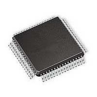
PIC18F65K90T-I/PT Microchip Technology, PIC18F65K90T-I/PT Datasheet - Page 385

PIC18F65K90T-I/PT
Manufacturer Part Number
PIC18F65K90T-I/PT
Description
32kB Flash, 2kB RAM, 1kB EE, NanoWatt XLP, LCD 64 TQFP 10x10x1mm T/R
Manufacturer
Microchip Technology
Series
PIC® XLP™ 18Fr
Datasheet
1.PIC18F66K90-IMR.pdf
(570 pages)
Specifications of PIC18F65K90T-I/PT
Processor Series
PIC18F
Core
PIC
Data Bus Width
8 bit
Program Memory Type
Flash
Program Memory Size
32 KB
Data Ram Size
2 KB
Interface Type
I2C, SPI
Maximum Clock Frequency
64 MHz
Number Of Timers
8
Operating Supply Voltage
1.8 V to 5.5 V
Maximum Operating Temperature
+ 125 C
3rd Party Development Tools
52715-96, 52716-328, 52717-734, 52712-325, EWPIC18
Minimum Operating Temperature
- 40 C
On-chip Adc
12 bit, 16 Channel
Core Processor
PIC
Core Size
8-Bit
Speed
64MHz
Connectivity
I²C, LIN, SPI, UART/USART
Peripherals
Brown-out Detect/Reset, LCD, POR, PWM, WDT
Number Of I /o
53
Eeprom Size
1K x 8
Ram Size
2K x 8
Voltage - Supply (vcc/vdd)
1.8 V ~ 5.5 V
Data Converters
A/D 16x12b
Oscillator Type
Internal
Operating Temperature
-40°C ~ 85°C
Package / Case
64-TQFP
Lead Free Status / Rohs Status
Details
Available stocks
Company
Part Number
Manufacturer
Quantity
Price
Company:
Part Number:
PIC18F65K90T-I/PT
Manufacturer:
Microchip Technology
Quantity:
10 000
Company:
Part Number:
PIC18F65K90T-I/PTRSL
Manufacturer:
Microchip Technology
Quantity:
10 000
- Current page: 385 of 570
- Download datasheet (5Mb)
23.4
The ADCON2 register allows the user to select an
acquisition time that occurs each time the GO/DONE
bit is set.
When the GO/DONE bit is set, sampling is stopped and
a conversion begins. The user is responsible for ensur-
ing the required acquisition time has passed between
selecting the desired input channel and setting the
GO/DONE bit.
This
(ADCON2<5:3>) remain in their Reset state (‘ 000 ’),
which is compatible with devices that do not offer
programmable acquisition times.
If desired, the ACQTx bits can be set to select a pro-
grammable acquisition time for the A/D module. When
the GO/DONE bit is set, the A/D module continues to
sample the input for the selected acquisition time, then
automatically begins a conversion. Since the acquisi-
tion time is programmed, there may be no need to wait
for an acquisition time between selecting a channel and
setting the GO/DONE bit.
In either case, when the conversion is completed, the
GO/DONE bit is cleared, the ADIF flag is set and the
A/D begins sampling the currently selected channel
again. If an acquisition time is programmed, there is
nothing to indicate if the acquisition time has ended or
if the conversion has begun.
23.5
The A/D conversion time per bit is defined as T
A/D conversion requires 14 T
The
software-selectable.
The possible options for T
• 2 T
• 4 T
• 8 T
• 16 T
• 32 T
• 64 T
• Using the internal RC Oscillator
For correct A/D conversions, the A/D conversion clock
(T
minimum
Parameter
Table 23-1
the device operating frequencies and the A/D clock
source selected.
2009-2011 Microchip Technology Inc.
AD
) must be as short as possible but greater than the
OSC
OSC
OSC
source
OSC
OSC
OSC
occurs
Selecting and Configuring
Automatic Acquisition Time
Selecting the A/D Conversion
Clock
130
shows the resultant T
T
AD
of
in
.
Table
when
the
(For
31-26.)
A/D
AD
more
the
are:
AD
conversion
per 12-bit conversion.
AD
ACQT<2:0>
times derived from
information,
clock
AD
. The
see
bits
is
PIC18F87K90 FAMILY
TABLE 23-1:
23.6
The ANCON0, ANCON1, ANCON2, TRISA, TRISF,
TRISG and TRISH registers control the operation of the
A/D port pins. The port pins needed as analog inputs
must have their corresponding TRISx bits set (input). If
the TRISx bit is cleared (output), the digital output level
(V
The A/D operation is independent of the state of the
CHS<3:0> bits and the TRISx bits.
2 T
4 T
8 T
16 T
32 T
64 T
RC
Note 1:
Operation
OH
Note 1: When reading the PORT register, all pins
OSC
OSC
OSC
(2)
AD Clock Source (T
OSC
OSC
OSC
or V
2:
Configuring Analog Port Pins
2: Analog levels on any pin defined as a
OL
The RC source has a typical T
4 s.
For device frequencies above 1 MHz, the
device must be in Sleep mode for the
entire conversion or the A/D accuracy
may be out of specification.
) will be converted.
configured as analog input channels will
read as cleared (a low level). Pins config-
ured as digital inputs will convert an
analog input. Analog levels on a digitally
configured
converted.
digital input may cause the digital input
buffer to consume current out of the
device’s specification limits.
T
FREQUENCIES
ADCS<2:0>
AD
000
100
001
101
010
110
x11
vs. DEVICE OPERATING
input
AD
)
will
Maximum Device
DS39957D-page 385
be
Frequency
10.00 MHz
20.00 MHz
40.00 MHz
64.00 MHz
1.00 MHz
2.50 MHz
5.00 MHz
AD
accurately
time of
(1)
Related parts for PIC18F65K90T-I/PT
Image
Part Number
Description
Manufacturer
Datasheet
Request
R

Part Number:
Description:
Manufacturer:
Microchip Technology Inc.
Datasheet:

Part Number:
Description:
Manufacturer:
Microchip Technology Inc.
Datasheet:

Part Number:
Description:
Manufacturer:
Microchip Technology Inc.
Datasheet:

Part Number:
Description:
Manufacturer:
Microchip Technology Inc.
Datasheet:

Part Number:
Description:
Manufacturer:
Microchip Technology Inc.
Datasheet:

Part Number:
Description:
Manufacturer:
Microchip Technology Inc.
Datasheet:

Part Number:
Description:
Manufacturer:
Microchip Technology Inc.
Datasheet:

Part Number:
Description:
Manufacturer:
Microchip Technology Inc.
Datasheet:


