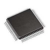
PIC18F65K90T-I/PT Microchip Technology, PIC18F65K90T-I/PT Datasheet - Page 412

PIC18F65K90T-I/PT
Manufacturer Part Number
PIC18F65K90T-I/PT
Description
32kB Flash, 2kB RAM, 1kB EE, NanoWatt XLP, LCD 64 TQFP 10x10x1mm T/R
Manufacturer
Microchip Technology
Series
PIC® XLP™ 18Fr
Datasheet
1.PIC18F66K90-IMR.pdf
(570 pages)
Specifications of PIC18F65K90T-I/PT
Processor Series
PIC18F
Core
PIC
Data Bus Width
8 bit
Program Memory Type
Flash
Program Memory Size
32 KB
Data Ram Size
2 KB
Interface Type
I2C, SPI
Maximum Clock Frequency
64 MHz
Number Of Timers
8
Operating Supply Voltage
1.8 V to 5.5 V
Maximum Operating Temperature
+ 125 C
3rd Party Development Tools
52715-96, 52716-328, 52717-734, 52712-325, EWPIC18
Minimum Operating Temperature
- 40 C
On-chip Adc
12 bit, 16 Channel
Core Processor
PIC
Core Size
8-Bit
Speed
64MHz
Connectivity
I²C, LIN, SPI, UART/USART
Peripherals
Brown-out Detect/Reset, LCD, POR, PWM, WDT
Number Of I /o
53
Eeprom Size
1K x 8
Ram Size
2K x 8
Voltage - Supply (vcc/vdd)
1.8 V ~ 5.5 V
Data Converters
A/D 16x12b
Oscillator Type
Internal
Operating Temperature
-40°C ~ 85°C
Package / Case
64-TQFP
Lead Free Status / Rohs Status
Details
Available stocks
Company
Part Number
Manufacturer
Quantity
Price
Company:
Part Number:
PIC18F65K90T-I/PT
Manufacturer:
Microchip Technology
Quantity:
10 000
Company:
Part Number:
PIC18F65K90T-I/PTRSL
Manufacturer:
Microchip Technology
Quantity:
10 000
- Current page: 412 of 570
- Download datasheet (5Mb)
PIC18F87K90 FAMILY
27.2.5
The CTMU sets its interrupt flag (PIR3<3>) whenever
the current source is enabled, then disabled. An inter-
rupt is generated only if the corresponding interrupt
enable bit (PIE3<3>) is also set. If edge sequencing is
not enabled (i.e., Edge 1 must occur before Edge 2), it
is necessary to monitor the edge status bits and
determine which edge occurred last and caused the
interrupt.
27.3
The following sequence is a general guideline used to
initialize the CTMU module:
1.
2.
3.
4.
5.
6.
7.
8.
9.
10. Disable the module by clearing the CTMUEN bit
11. Clear the Edge Status bits, EDG2STAT and
12. Enable both edge inputs by setting the EDGEN
13. Enable the module by setting the CTMUEN bit.
DS39957D-page 412
Select the current source range using the
IRNGx bits (CTMUICON<1:0>).
Adjust the current source trim using the ITRIMx
bits (CTMUICON<7:2>).
Configure the edge input sources for Edge 1 and
Edge 2 by setting the EDG1SEL and EDG2SEL
bits (CTMUCONL<3:2> and <6:5>, respectively).
Configure the input polarities for the edge inputs
using the EDG2POL and EDG1POL bits
(CTMUCONL<7,4>).
The default configuration is for negative edge
polarity (high-to-low transitions).
Enable edge sequencing using the EDGSEQEN
bit (CTMUCONH<2>).
By default, edge sequencing is disabled.
Select the operating mode (Measurement or
Time Delay) with the TGEN bit.
The default mode is the Time/Capacitance
Measurement.
Configure the module to automatically trigger
an A/D conversion when the second edge
event has occurred using the CTTRIG bit
(CTMUCONH<0>).
The conversion trigger is disabled by default.
Discharge the connected circuit by setting the
IDISSEN bit (CTMUCONH<1>).
After waiting a sufficient time for the circuit to
discharge, clear IDISSEN.
(CTMUCONH<7>).
EDG1STAT (CTMUCONL<1:0>).
bit (CTMUCONH<3>).
CTMU Module Initialization
INTERRUPTS
Depending on the type of measurement or pulse
generation being performed, one or more additional
modules may also need to be initialized and configured
with the CTMU module:
• Edge Source Generation: In addition to the
• Capacitance or Time Measurement: The CTMU
• Pulse Generation: When generating system clock
27.4
The CTMU requires calibration for precise measure-
ments of capacitance and time, as well as for accurate
time delay. If the application only requires measurement
of a relative change in capacitance or time, calibration is
usually not necessary. An example of a lesser precision
application is a capacitive touch switch, in which the
touch circuit has a baseline capacitance and the added
capacitance of the human body changes the overall
capacitance of a circuit.
If actual capacitance or time measurement is required,
two hardware calibrations must take place:
• The current source needs calibration to set it to a
• The circuit being measured needs calibration to
27.4.1
The current source on board the CTMU module has a
range of ±60% nominal for each of three current
ranges. For precise measurements, it is possible to
measure and adjust this current source by placing a
high-precision resistor, R
channel. An example circuit is shown in
To measure the current source:
1.
2.
3.
4.
5.
6.
external edge input pins, CCPx Special Event
Triggers can be used as edge sources for the
CTMU.
module uses the A/D Converter to measure the
voltage across a capacitor that is connected to one
of the analog input channels.
independent, output pulses, the CTMU module
uses Comparator 2 and the associated
comparator voltage reference.
precise current.
measure or nullify any capacitance other than that
to be measured.
Initialize the A/D Converter.
Initialize the CTMU.
Enable the current source by setting EDG1STAT
(CTMUCONL<0>).
Issue the settling time delay.
Perform the A/D conversion.
Calculate the current source current using
I = V/R
resistance and V is measured by performing an
A/D conversion.
Calibrating the CTMU Module
CAL
CURRENT SOURCE CALIBRATION
, where R
2009-2011 Microchip Technology Inc.
CAL
CAL
, onto an unused analog
is a high-precision
Figure
27-2.
Related parts for PIC18F65K90T-I/PT
Image
Part Number
Description
Manufacturer
Datasheet
Request
R

Part Number:
Description:
Manufacturer:
Microchip Technology Inc.
Datasheet:

Part Number:
Description:
Manufacturer:
Microchip Technology Inc.
Datasheet:

Part Number:
Description:
Manufacturer:
Microchip Technology Inc.
Datasheet:

Part Number:
Description:
Manufacturer:
Microchip Technology Inc.
Datasheet:

Part Number:
Description:
Manufacturer:
Microchip Technology Inc.
Datasheet:

Part Number:
Description:
Manufacturer:
Microchip Technology Inc.
Datasheet:

Part Number:
Description:
Manufacturer:
Microchip Technology Inc.
Datasheet:

Part Number:
Description:
Manufacturer:
Microchip Technology Inc.
Datasheet:


