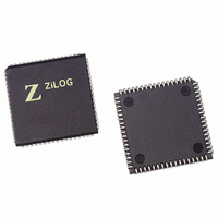
Z16C3510VSG Zilog, Z16C3510VSG Datasheet - Page 41

Z16C3510VSG
Manufacturer Part Number
Z16C3510VSG
Description
IC 10MHZ Z8500 CMOS ISCC 68-PLCC
Manufacturer
Zilog
Series
IUSC™r
Specifications of Z16C3510VSG
Controller Type
Serial Communications Controller (SCC)
Interface
USB
Voltage - Supply
4.75 V ~ 5.25 V
Current - Supply
50mA
Operating Temperature
0°C ~ 70°C
Mounting Type
Surface Mount
Package / Case
68-LCC (J-Lead)
Lead Free Status / RoHS Status
Lead free / RoHS Compliant
Available stocks
Company
Part Number
Manufacturer
Quantity
Price
- Current page: 41 of 268
- Download datasheet (3Mb)
not debounced to generate breaks. Switch bounce may
cause multiple breaks, recognized by the ISCC to be addi-
tional characters assembled in the receive data FIFO. It
may also cause a receive overrun condition being latched.
Received characters are assembled, checked for errors,
and moved to a three byte FIFO. When there is at least
one character in the FIFO the Rx Character Available bit
(in RR0) is set to 1 and, optionally, an interrupt or DMA re-
quest can be generated. Since errors apply to specific
characters, it is necessary that error information moves
along side the data that it refers to. This is implemented in
the ISCC with a three entry error FIFO in parallel with the
data FIFO. The three error conditions that the receiver
checks for in asynchronous mode are:
1. Framing errors - when a character stop bit is found to
2. Parity errors - when parity is enabled and the parity of
3. Overrun errors - when the FIFO overflows.
4.3 BYTE-ORIENTED SYNCHRONOUS MODE
Three byte-oriented synchronous protocols supported by
ISCC are monosync, bisync, and external sync.
In synchronous communications the bit cell boundaries
are defined by a clock signal which is common to both the
transmitter and receiver. Of course there must also be an
agreement as to the location of the character boundaries
so that the characters can be properly framed. This is nor-
mally accomplished by defining special SYNC patterns, or
SYNC characters. The SYNC pattern serves as a refer-
ence; it signals the receiver that a character boundary oc-
curs immediately after the last bit of the pattern. Another
way of identifying the character boundaries (i.e., achieving
synchronization) is with a logic signal that goes active just
as the first character is about to enter the receiver. This
method is referred to as “External Synchronization”.
UM011001-0601
be 0.
a character disagrees with the sense programmed in
WR4.
The initialization sequence for the receiver in asynchro-
nous mode is given in Table 4-4 below.
Note: * Initializes transmitter and receiver simultaneously
At this point other registers should be initialized according
to the hardware design such as clocking, I/O mode, etc.
When all this is completed, the receiver may be enabled by
setting WR3(0) = 1. Also note that the transmitter and re-
ceiver may be initialized at the same time.
Figure 4-4 shows the character format for synchronous
transmission. For example, bits 1-8 might be one character
and bits 9-13 part of another character; or bit 1 might be part
of a second character, and bits 10-13 part of a third
character. The alignment of the received bytes to the byte
assembly is accomplished by defining a synchronization
character, commonly called a “sync character”.
Table 4-4. Initialization Sequence for the Receiver
WR4
WR3
WR5
Reg
Bit No
3, 2
0, 1
6, 7
7, 6
5
1
in Asynchronous Mode
Description
Select Async Mode and the number
of stop bits*
Select parity*
Select clock mode*
Select number of bits/character
Select Auto Enable Mode*
Select modem control (RTS)
Z16C35ISCC™ User’s Manual
Data Communication Modes
4-7
4
Related parts for Z16C3510VSG
Image
Part Number
Description
Manufacturer
Datasheet
Request
R

Part Number:
Description:
CMOS ISCC INTEGRATED SERIAL COMMUNICATIONS CONTROLLER
Manufacturer:
ZILOG [Zilog, Inc.]
Datasheet:

Part Number:
Description:
Communication Controllers, ZILOG INTELLIGENT PERIPHERAL CONTROLLER (ZIP)
Manufacturer:
Zilog, Inc.
Datasheet:

Part Number:
Description:
KIT DEV FOR Z8 ENCORE 16K TO 64K
Manufacturer:
Zilog
Datasheet:

Part Number:
Description:
KIT DEV Z8 ENCORE XP 28-PIN
Manufacturer:
Zilog
Datasheet:

Part Number:
Description:
DEV KIT FOR Z8 ENCORE 8K/4K
Manufacturer:
Zilog
Datasheet:

Part Number:
Description:
KIT DEV Z8 ENCORE XP 28-PIN
Manufacturer:
Zilog
Datasheet:

Part Number:
Description:
DEV KIT FOR Z8 ENCORE 4K TO 8K
Manufacturer:
Zilog
Datasheet:

Part Number:
Description:
CMOS Z8 microcontroller. ROM 16 Kbytes, RAM 256 bytes, speed 16 MHz, 32 lines I/O, 3.0V to 5.5V
Manufacturer:
Zilog, Inc.
Datasheet:

Part Number:
Description:
Low-cost microcontroller. 512 bytes ROM, 61 bytes RAM, 8 MHz
Manufacturer:
Zilog, Inc.
Datasheet:

Part Number:
Description:
Z8 4K OTP Microcontroller
Manufacturer:
Zilog, Inc.
Datasheet:

Part Number:
Description:
CMOS SUPER8 ROMLESS MCU
Manufacturer:
Zilog, Inc.
Datasheet:

Part Number:
Description:
SL1866 CMOSZ8 OTP Microcontroller
Manufacturer:
Zilog, Inc.
Datasheet:

Part Number:
Description:
SL1866 CMOSZ8 OTP Microcontroller
Manufacturer:
Zilog, Inc.
Datasheet:

Part Number:
Description:
OTP (KB) = 1, RAM = 125, Speed = 12, I/O = 14, 8-bit Timers = 2, Comm Interfaces Other Features = Por, LV Protect, Voltage = 4.5-5.5V
Manufacturer:
Zilog, Inc.
Datasheet:


