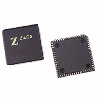
Z16C3510VSG Zilog, Z16C3510VSG Datasheet - Page 87

Z16C3510VSG
Manufacturer Part Number
Z16C3510VSG
Description
IC 10MHZ Z8500 CMOS ISCC 68-PLCC
Manufacturer
Zilog
Series
IUSC™r
Specifications of Z16C3510VSG
Controller Type
Serial Communications Controller (SCC)
Interface
USB
Voltage - Supply
4.75 V ~ 5.25 V
Current - Supply
50mA
Operating Temperature
0°C ~ 70°C
Mounting Type
Surface Mount
Package / Case
68-LCC (J-Lead)
Lead Free Status / RoHS Status
Lead free / RoHS Compliant
Available stocks
Company
Part Number
Manufacturer
Quantity
Price
- Current page: 87 of 268
- Download datasheet (3Mb)
UM011001-0601
Bit 5 selects the no vector option. With this bit set, the DMA
cell does not return an interrupt vector to the CPU. During
the interrupt acknowledge cycle when the interrupt vector
is requested, the ISCC will not drive the bus. With this bit
clear, an interrupt vector will be returned in the interrupt ac-
knowledge cycle.
Bit 4 selects the vector include status option for the inter-
rupt vector from the DMA cell. With this bit clear, a DMA in-
terrupt vector will be returned which is the vector that has
been programmed into the Interrupt Vector Register. With
this bit set, the returned vector contains status information
concerning the interrupt source. The status returned re-
flects the highest priority interrupt pending (IP bit is set and
the corresponding Interrupt Enable bit is set). This status
information is contained in bits 1, 2, and 3 of the interrupt
vector. The other interrupt vector bits remain unmodified.
Bit 3, when set, enables the interrupt from the Receiver A
DMA.
Bit 2, when set, enables the interrupt from the Transmitter
A DMA.
Bit 1, when set, enables the interrupt from the Receiver B
DMA.
Bit 0, when set, enables the interrupt from the Transmitter
B DMA.
5.6.4 Interrupt Vector Register
This register holds the interrupt vector for the DMA cell.
The value programmed into this register is returned during
the interrupt response cycle as the interrupt vector when
one of the DMA interrupt sources is the highest priority
pending interrupt. Note that bits 1, 2, and 3 may be re-
placed by interrupt status information if the Vector Include
Status option has been selected (see Interrupt Control
Register). The bit positions are shown in Figure 5-29.
IV3
0
0
0
0
1
1
1
1
Table 5-14. Interrupt Vector Status Encoding
IV2
0
0
1
1
0
0
1
1
IV1
0
1
0
1
0
1
0
1
Interrupt
No Interrupt Pending
Not Possible
Not Possible
Not Possible
Rx A IP
Rx B IP
Tx A IP
Tx B IP
P R E L I M I N A R Y
5.6.5 Interrupt Command Register
This is a write only register and is used to command the
DMA cell. It shares its address with the Interrupt Status
Register. The bit positions for the Interrupt Command Reg-
ister are shown in Figure 5-30.
Bits 7 through 5 are encoded with the commands for the
DMA cell as shown below:
Bit combination 000 is a Null command and has no affect
on the DMA.
Address: 00011 (Write)
D7
0
0
0
0
1
1
1
1
Figure 5-30. Interrupt Command Register
Figure 5-29. Interrupt Vector Register
D6
Address: 00010
0
0
1
1
0
0
1
1
D7
* Potentially modified by interrupt condition
D5 D4 D3 D2 D1 D0
0
1
0
1
0
1
0
1
D6
DMA Interrupt Commands
D5 D4 D3 D2 D1 D0
Null Comand
Reset IP
Reset IUS
Reset IP and IUS
Reserved
Set IP
Set IUS
Set IP and IUS
Z16C35ISCC™ User’s Manual
Register Descriptions
Select Tx B DMA
Select Rx B DMA
Select Tx A DMA
Select Rx A DMA
Reserved
IV2
IV0
IV1
IV3
IV4
IV5
IV6
IV7
*
5-27
5
Related parts for Z16C3510VSG
Image
Part Number
Description
Manufacturer
Datasheet
Request
R

Part Number:
Description:
CMOS ISCC INTEGRATED SERIAL COMMUNICATIONS CONTROLLER
Manufacturer:
ZILOG [Zilog, Inc.]
Datasheet:

Part Number:
Description:
Communication Controllers, ZILOG INTELLIGENT PERIPHERAL CONTROLLER (ZIP)
Manufacturer:
Zilog, Inc.
Datasheet:

Part Number:
Description:
KIT DEV FOR Z8 ENCORE 16K TO 64K
Manufacturer:
Zilog
Datasheet:

Part Number:
Description:
KIT DEV Z8 ENCORE XP 28-PIN
Manufacturer:
Zilog
Datasheet:

Part Number:
Description:
DEV KIT FOR Z8 ENCORE 8K/4K
Manufacturer:
Zilog
Datasheet:

Part Number:
Description:
KIT DEV Z8 ENCORE XP 28-PIN
Manufacturer:
Zilog
Datasheet:

Part Number:
Description:
DEV KIT FOR Z8 ENCORE 4K TO 8K
Manufacturer:
Zilog
Datasheet:

Part Number:
Description:
CMOS Z8 microcontroller. ROM 16 Kbytes, RAM 256 bytes, speed 16 MHz, 32 lines I/O, 3.0V to 5.5V
Manufacturer:
Zilog, Inc.
Datasheet:

Part Number:
Description:
Low-cost microcontroller. 512 bytes ROM, 61 bytes RAM, 8 MHz
Manufacturer:
Zilog, Inc.
Datasheet:

Part Number:
Description:
Z8 4K OTP Microcontroller
Manufacturer:
Zilog, Inc.
Datasheet:

Part Number:
Description:
CMOS SUPER8 ROMLESS MCU
Manufacturer:
Zilog, Inc.
Datasheet:

Part Number:
Description:
SL1866 CMOSZ8 OTP Microcontroller
Manufacturer:
Zilog, Inc.
Datasheet:

Part Number:
Description:
SL1866 CMOSZ8 OTP Microcontroller
Manufacturer:
Zilog, Inc.
Datasheet:

Part Number:
Description:
OTP (KB) = 1, RAM = 125, Speed = 12, I/O = 14, 8-bit Timers = 2, Comm Interfaces Other Features = Por, LV Protect, Voltage = 4.5-5.5V
Manufacturer:
Zilog, Inc.
Datasheet:


