DP83849CVS/NOPB National Semiconductor, DP83849CVS/NOPB Datasheet - Page 12
DP83849CVS/NOPB
Manufacturer Part Number
DP83849CVS/NOPB
Description
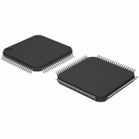
IC TXRX ETHERNET PHY DUAL 80TQFP
Manufacturer
National Semiconductor
Type
Transceiverr
Specifications of DP83849CVS/NOPB
Number Of Drivers/receivers
2/2
Protocol
Ethernet
Voltage - Supply
3 V ~ 3.6 V
Mounting Type
Surface Mount
Package / Case
80-TQFP, 80-VQFP
Data Rate
100Mbps
Supply Voltage Range
3V To 3.6V
Logic Case Style
TQFP
No. Of Pins
80
Operating Temperature Range
0°C To +70°C
Msl
MSL 3 - 168 Hours
Filter Terminals
SMD
Rohs Compliant
Yes
Data Rate Max
10Mbps
For Use With
DP83849CVS-EVK - BOARD EVALUATION DP83849CVS
Lead Free Status / RoHS Status
Lead free / RoHS Compliant
Other names
*DP83849CVS
*DP83849CVS/NOPB
DP83849CVS
*DP83849CVS/NOPB
DP83849CVS
Available stocks
Company
Part Number
Manufacturer
Quantity
Price
Company:

Part Number:
DP83849CVS/NOPB
Manufacturer:
NS
Quantity:
618
Company:
Part Number:
DP83849CVS/NOPB
Manufacturer:
Texas Instruments
Quantity:
10 000


www.national.com
1.3 Clock Interface
1.4 LED Interface
The DP83849I supports three configurable LED pins. The
LEDs support two operational modes which are selected
by the LED mode strap and a third operational mode which
X1
X2
CLK2MAC
LED_LINK_A
LED_LINK_B
LED_SPEED_A
LED_SPEED_B
LED_ACT/LED_COL_A
LED_ACT/LED_COL_B
Signal Name
Signal Name
Type
Type
I/O
I/O
I/O
O
O
I
Pin #
Pin #
70
69
68
19
43
20
42
21
41
CRYSTAL/OSCILLATOR INPUT: This pin is the primary clock
reference input for the DP83849I and must be connected to a 25
MHz 0.005% (+50 ppm) clock source. The DP83849I supports ei-
ther an external crystal resonator connected across pins X1 and
X2, or an external CMOS-level oscillator source connected to pin
X1 only.
RMII REFERENCE CLOCK: This pin is the primary clock refer-
ence input for the RMII mode and must be connected to a 50 MHz
0.005% (+50 ppm) CMOS-level oscillator source.
CRYSTAL OUTPUT: This pin is the primary clock reference out-
put to connect to an external 25 MHz crystal resonator device.
This pin must be left unconnected if an external CMOS oscillator
clock source is used.
CLOCK TO MAC:
In MII mode, this pin provides a 25 MHz clock output to the sys-
tem.
In RMII mode, this pin provides a 50 MHz clock output to the sys-
tem.
This allows other devices to use the reference clock from the
DP83849I without requiring additional clock sources.
If the system does not require the CLK2MAC signal, the
CLK2MAC output should be disabled via the CLK2MAC disable
strap.
LINK LED: In Mode 1, this pin indicates the status of the LINK.
The LED will be ON when Link is good.
LINK/ACT LED: In Mode 2 and Mode 3, this pin indicates transmit
and receive activity in addition to the status of the Link. The LED
will be ON when Link is good. It will blink when the transmitter or
receiver is active.
SPEED LED: The LED is ON when device is in 100 Mb/s and OFF
when in 10 Mb/s. Functionality of this LED is independent of mode
selected.
ACTIVITY LED: In Mode 1, this pin is the Activity LED which is
ON when activity is present on either Transmit or Receive.
COLLISION/DUPLEX LED: In Mode 2, this pin by default indi-
cates Collision detection. For Mode 3, this LED output may be
programmed to indicate Full-duplex status instead of Collision.
12
is register configurable. The definitions for the LEDs for
each mode are detailed below. Since the LEDs are also
used as strap options, the polarity of the LED output is
dependent on whether the pin is pulled up or down.
Description
Description
Related parts for DP83849CVS/NOPB
Image
Part Number
Description
Manufacturer
Datasheet
Request
R

Part Number:
Description:
National Semiconductor [8-Bit D/A Converter]
Manufacturer:
National Semiconductor
Datasheet:
Part Number:
Description:
National Semiconductor [Media Coprocessor]
Manufacturer:
National Semiconductor
Datasheet:
Part Number:
Description:
Digitally Controlled Tone and Volume Circuit with Stereo Audio Power Amplifier, Microphone Preamp Stage and National 3D Sound
Manufacturer:
National Semiconductor
Datasheet:
Part Number:
Description:
Digitally Controlled Tone and Volume Circuit with Stereo Audio Power Amplifier, Microphone Preamp Stage and National 3D Sound
Manufacturer:
National Semiconductor
Datasheet:
Part Number:
Description:
AC97 Rev 2 Codec with Sample Rate Conversion and National 3D Sound
Manufacturer:
National Semiconductor
Part Number:
Description:
Manufacturer:
National Semiconductor
Datasheet:
Part Number:
Description:
Manufacturer:
National Semiconductor
Datasheet:
Part Number:
Description:
General Purpose, Low Voltage, Low Power, Rail-to-Rail Output Operational Amplifiers
Manufacturer:
National Semiconductor
Datasheet:
Part Number:
Description:
8-bit 20 MSPS flash A/D converter.
Manufacturer:
National Semiconductor
Datasheet:
Part Number:
Description:
Low Noise Quad Operational Amplifier
Manufacturer:
National Semiconductor
Datasheet:
Part Number:
Description:
Quad Differential Line Receivers
Manufacturer:
National Semiconductor
Datasheet:
Part Number:
Description:
Quad High Speed Trapezoidal? Bus Transceiver
Manufacturer:
National Semiconductor
Datasheet:
Part Number:
Description:
Dual Line Receiver
Manufacturer:
National Semiconductor
Datasheet:
Part Number:
Description:
TTL to 10k ECL Level Translator with Latch
Manufacturer:
National Semiconductor
Datasheet: