DP83849CVS/NOPB National Semiconductor, DP83849CVS/NOPB Datasheet - Page 25
DP83849CVS/NOPB
Manufacturer Part Number
DP83849CVS/NOPB
Description
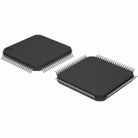
IC TXRX ETHERNET PHY DUAL 80TQFP
Manufacturer
National Semiconductor
Type
Transceiverr
Specifications of DP83849CVS/NOPB
Number Of Drivers/receivers
2/2
Protocol
Ethernet
Voltage - Supply
3 V ~ 3.6 V
Mounting Type
Surface Mount
Package / Case
80-TQFP, 80-VQFP
Data Rate
100Mbps
Supply Voltage Range
3V To 3.6V
Logic Case Style
TQFP
No. Of Pins
80
Operating Temperature Range
0°C To +70°C
Msl
MSL 3 - 168 Hours
Filter Terminals
SMD
Rohs Compliant
Yes
Data Rate Max
10Mbps
For Use With
DP83849CVS-EVK - BOARD EVALUATION DP83849CVS
Lead Free Status / RoHS Status
Lead free / RoHS Compliant
Other names
*DP83849CVS
*DP83849CVS/NOPB
DP83849CVS
*DP83849CVS/NOPB
DP83849CVS
Available stocks
Company
Part Number
Manufacturer
Quantity
Price
Company:

Part Number:
DP83849CVS/NOPB
Manufacturer:
NS
Quantity:
618
Company:
Part Number:
DP83849CVS/NOPB
Manufacturer:
Texas Instruments
Quantity:
10 000


3.3 10 Mb Serial Network Interface (SNI)
The DP83849I incorporates a 10 Mb Serial Network Inter-
face (SNI) which allows a simple serial data interface for 10
Mb only devices. This is also referred to as a 7-wire inter-
face. While there is no defined standard for this interface, it
is based on early 10 Mb physical layer devices. Data is
clocked serially at 10 MHz using separate transmit and
receive paths. The following pins are used in SNI mode:
— TX_CLK
— TX_EN
— TXD[0]
— RX_CLK
— RXD[0]
— CRS
— COL
Start Threshold
01 (default)
RBR[1:0]
10
11
00
Table 5. Supported SCMII packet sizes at +/-50ppm frequency accuracy
100Mb
12 bits
12 bits
4 bits
4 bits
Latency Tolerance
10Mb
8 bits
8 bits
8 bits
8 bits
25
3.4 Single Clock MII Mode
Single Clock MII (SCMII) Mode allows MII operation using
a single 25MHz reference clock. Normal MII Mode requires
three clocks, a reference clock for physical layer functions,
a Transmit MII clock, and a Receive MII clock. Similar to
RMII mode, Single Clock MII mode requires only the refer-
ence clock. In addition to reducing the number of pins
required, this mode allows the attached MAC device to use
only the reference clock domain. Since the DP83849I has
two ports, this actually reduces the number of clocks from 6
to 1. A/C Timing requirements for SCMII operation are
similar to the RMII timing requirements.
For 10Mb operation, as in RMII mode, data is sampled and
driven every 10 clocks since the reference clock is at 10x
the data rate.
Separate control bits allow enabling the Transmit and
Receive Single Clock modes separately, allowing just
transmit or receive to operate in this mode. Control of Sin-
gle Clock MII mode is through the RBR register.
Single Clock MII mode incorporates the use of the RMII
elasticity buffer, which is required to tolerate potential fre-
quency differences between the 25MHz reference clock
and the recovered receive clock. Settings for the Elasticity
Buffer for SCMII mode are detailed in the following table.
4,000 bytes
4,000 bytes
9.600 bytes
9,600 bytes
100Mb
Recommended Packet Size
at +/- 50ppm
9,600 bytes
9,600 bytes
9,600 bytes
9,600 bytes
www.national.com
10Mb
Related parts for DP83849CVS/NOPB
Image
Part Number
Description
Manufacturer
Datasheet
Request
R

Part Number:
Description:
National Semiconductor [8-Bit D/A Converter]
Manufacturer:
National Semiconductor
Datasheet:
Part Number:
Description:
National Semiconductor [Media Coprocessor]
Manufacturer:
National Semiconductor
Datasheet:
Part Number:
Description:
Digitally Controlled Tone and Volume Circuit with Stereo Audio Power Amplifier, Microphone Preamp Stage and National 3D Sound
Manufacturer:
National Semiconductor
Datasheet:
Part Number:
Description:
Digitally Controlled Tone and Volume Circuit with Stereo Audio Power Amplifier, Microphone Preamp Stage and National 3D Sound
Manufacturer:
National Semiconductor
Datasheet:
Part Number:
Description:
AC97 Rev 2 Codec with Sample Rate Conversion and National 3D Sound
Manufacturer:
National Semiconductor
Part Number:
Description:
Manufacturer:
National Semiconductor
Datasheet:
Part Number:
Description:
Manufacturer:
National Semiconductor
Datasheet:
Part Number:
Description:
General Purpose, Low Voltage, Low Power, Rail-to-Rail Output Operational Amplifiers
Manufacturer:
National Semiconductor
Datasheet:
Part Number:
Description:
8-bit 20 MSPS flash A/D converter.
Manufacturer:
National Semiconductor
Datasheet:
Part Number:
Description:
Low Noise Quad Operational Amplifier
Manufacturer:
National Semiconductor
Datasheet:
Part Number:
Description:
Quad Differential Line Receivers
Manufacturer:
National Semiconductor
Datasheet:
Part Number:
Description:
Quad High Speed Trapezoidal? Bus Transceiver
Manufacturer:
National Semiconductor
Datasheet:
Part Number:
Description:
Dual Line Receiver
Manufacturer:
National Semiconductor
Datasheet:
Part Number:
Description:
TTL to 10k ECL Level Translator with Latch
Manufacturer:
National Semiconductor
Datasheet: