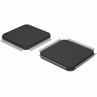
DP83849CVS/NOPB National Semiconductor, DP83849CVS/NOPB Datasheet - Page 13

DP83849CVS/NOPB
Manufacturer Part Number
DP83849CVS/NOPB
Description
IC TXRX ETHERNET PHY DUAL 80TQFP
Manufacturer
National Semiconductor
Type
Transceiverr
Specifications of DP83849CVS/NOPB
Number Of Drivers/receivers
2/2
Protocol
Ethernet
Voltage - Supply
3 V ~ 3.6 V
Mounting Type
Surface Mount
Package / Case
80-TQFP, 80-VQFP
Data Rate
100Mbps
Supply Voltage Range
3V To 3.6V
Logic Case Style
TQFP
No. Of Pins
80
Operating Temperature Range
0°C To +70°C
Msl
MSL 3 - 168 Hours
Filter Terminals
SMD
Rohs Compliant
Yes
Data Rate Max
10Mbps
For Use With
DP83849CVS-EVK - BOARD EVALUATION DP83849CVS
Lead Free Status / RoHS Status
Lead free / RoHS Compliant
Other names
*DP83849CVS
*DP83849CVS/NOPB
DP83849CVS
*DP83849CVS/NOPB
DP83849CVS
Available stocks
Company
Part Number
Manufacturer
Quantity
Price
Company:
Part Number:
DP83849CVS/NOPB
Manufacturer:
NS
Quantity:
618
Company:
Part Number:
DP83849CVS/NOPB
Manufacturer:
Texas Instruments
Quantity:
10 000
1.5 JTAG Interface
1.6 Reset and Power Down
1.7 Strap Options
The DP83849I uses many of the functional pins as strap
options. The values of these pins are sampled during reset
and used to strap the device into specific modes of opera-
tion. The strap option pin assignments are defined below.
The functional pin name is indicated in parentheses.
TCK
TDO
TMS
TRSTN
TDI
RESET_N
PWRDOWN_INT_A
PWRDOWN_INT_B
PHYAD1 (RXD0_A)
PHYAD2 (RXD1_A)
PHYAD3 (RXD0_B)
PHYAD4 (RXD1_B)
Signal Name
Signal Name
Signal Name
S, O, PD
S, O, PD
S, O, PD
S, O, PD
Type
Type
Type
I, PU
I, PU
I, PU
I, PU
I, PU
I, PU
O
Pin #
Pin #
Pin #
72
73
74
75
76
71
18
44
58
57
4
5
TEST CLOCK
This pin has a weak internal pullup.
TEST OUTPUT
TEST MODE SELECT
This pin has a weak internal pullup.
TEST RESET Active low test reset.
This pin has a weak internal pullup.
TEST DATA INPUT
This pin has a weak internal pullup.
RESET: Active Low input that initializes or re-initializes the
DP83849I. Asserting this pin low for at least 1 s will force a reset
process to occur. All internal registers will re-initialize to their de-
fault states as specified for each bit in the Register Block section.
All strap options are re-initialized as well.
The default function of this pin is POWER DOWN.
POWER DOWN: The pin is an active low input in this mode and
should be asserted low to put the device in a Power Down mode.
INTERRUPT: The pin is an open drain output in this mode and will
be asserted low when an interrupt condition occurs. Although the
pin has a weak internal pull-up, some applications may require an
external pull-up resister. Register access is required for the pin to
be used as an interrupt mechanism. See Section 5.5.2 Interrupt
Mechanism for more details on the interrupt mechanisms.
PHY ADDRESS [4:1]: The DP83849I provides four PHY address
pins, the state of which are latched into the PHYCTRL register at
system Hardware-Reset. Phy Address[0] selects between ports A
and B.
The DP83849I supports PHY Address strapping for Port A even
values 0 (<0000_0>) through 30 (<1111_0>). Port B will be
strapped to odd values 1 (<0000_1>) through 31 (<1111_1>).
PHYAD[4:1] pins have weak internal pull-down resistors.
13
A 2.2 k resistor should be used for pull-down or pull-up to
change the default strap option. If the default option is
required, then there is no need for external pull-up or pull
down resistors. Since these pins may have alternate func-
tions after reset is deasserted, they should not be con-
nected directly to VCC or GND.
Description
Description
Description
www.national.com


