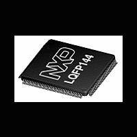
LPC2926_27_29 NXP Semiconductors, LPC2926_27_29 Datasheet - Page 43

LPC2926_27_29
Manufacturer Part Number
LPC2926_27_29
Description
The LPC2926/2927/2929 combine an ARM968E-S CPU core with two integrated TCMblocks operating at frequencies of up to 125 MHz, Full-speed USB 2
Manufacturer
NXP Semiconductors
Datasheet
1.LPC2926_27_29.pdf
(95 pages)
- Current page: 43 of 95
- Download datasheet (2Mb)
NXP Semiconductors
LPC2926_27_29
Product data sheet
6.15.4.3 Clock description
Table 23.
[1]
[2]
[3]
Remark: The following formula only applies to ADC0:
Voltage variations on VREFP (i.e. those that deviate from voltage variations on the
V
formula is used to determine the conversion result of an input voltage V
Remark: Note that the ADC1 and ADC2 accept an input voltage up to of 3.6 V (see
Table
ADC0 pins are 5 V tolerant.
The ADC modules are clocked from two different sources; CLK_MSCSS_ADCx_APB and
CLK_ADCx (x = 0, 1, or 2), see
CLK_ADCx and CLK_MSCSS_ADCx_APB branch clocks for power management. If an
ADC is unused both its CLK_MSCSS_ADCx_APB and CLK_ADCx can be switched off.
The frequency of all the CLK_MSCSS_ADCx_APB clocks is identical to
CLK_MSCSS_APB since they are derived from the same base clock
BASE_MSCSS_CLK. Likewise the frequency of all the CLK_ADCx clocks is identical
since they are derived from the same base clock BASE_ADC_CLK.
The register interface towards the system bus is clocked by CLK_MSCSS_ADCx_APB.
Control logic for the analog section of the ADC is clocked by CLK_ADCx, see also
Figure
Symbol
ADC0 IN[7:0]
ADC1/2 IN[7:0]
ADC2_EXT_START
VREFN
VREFP
V
V
⎛
⎝
DDA(ADC5V5)
DDA(ADC5V0)
DDA(ADC3V3)
2
-- - V
3
⎛
⎝
VREFP, VREFN, V
The analog inputs of ADC0 are internally multiplied by a factor of 3.3 / 5. If V
3.3 V, the maximum digital result is 1024 × 3.3 / 5.
V
DDA(ADC5V0)
I
34) on the ADC1/2 IN pins. If the ADC is not used, the pins are 5 V tolerant. The
–
9.
1
-- - V
2
ADC pins
DDA ADC5V0
pin) are visible as variations in the measurement result. The following
and V
(
All information provided in this document is subject to legal disclaimers.
DDA(ADC3V3)
DDA(ADC3V3)
Rev. 5 — 28 September 2010
Pin name
IN0[7:0]
IN1/2[7:0]
CAP1[2]
VREFN
VREFP
V
V
DDA(ADC5V0)
DDA(ADC3V3)
)
⎞
⎠
+
1
-- - V
2
must be connected for the 5 V ADC0 to operate properly.
must be set as follows: V
DDA ADC3V3
Section
[1]
(
IN
IN
IN
IN
IN
Direction Description
IN
IN
ARM9 microcontroller with CAN, LIN, and USB
6.7.2. Note that each ADC has its own
)
⎞
⎠
×
------------------------------------------- -
V
analog input for 5.0 V ADC0, channel 7 to
channel 0.
analog input for 3.3 V ADC1/2, channel 7 to
channel 0.
ADC external start-trigger input.
ADC LOW reference level.
ADC HIGH reference level.
5 V high-power supply and HIGH reference for
ADC0. Connect to clean 5 V as HIGH
reference. May also be connected to 3.3 V if
3.3 V measurement range for ADC0 is
needed.
ADC1 and ADC2 3.3 V supply (also used for
ADC0).
VREFP
LPC2926/2927/2929
DDA(ADC5V0)
1024
[3]
–
[2][3]
V
VREFN
= V
DDA(ADC3V3)
DDA(ADC5V0)
© NXP B.V. 2010. All rights reserved.
× 1.5.
I
on ADC0:
is connected to
43 of 95
(3)
Related parts for LPC2926_27_29
Image
Part Number
Description
Manufacturer
Datasheet
Request
R
Part Number:
Description:
Lpc2926/2927/2929 Arm9 Microcontroller With Can, Lin, And Usb
Manufacturer:
NXP Semiconductors
Datasheet:
Part Number:
Description:
NXP Semiconductors designed the LPC2420/2460 microcontroller around a 16-bit/32-bitARM7TDMI-S CPU core with real-time debug interfaces that include both JTAG andembedded trace
Manufacturer:
NXP Semiconductors
Datasheet:

Part Number:
Description:
NXP Semiconductors designed the LPC2458 microcontroller around a 16-bit/32-bitARM7TDMI-S CPU core with real-time debug interfaces that include both JTAG andembedded trace
Manufacturer:
NXP Semiconductors
Datasheet:
Part Number:
Description:
NXP Semiconductors designed the LPC2468 microcontroller around a 16-bit/32-bitARM7TDMI-S CPU core with real-time debug interfaces that include both JTAG andembedded trace
Manufacturer:
NXP Semiconductors
Datasheet:
Part Number:
Description:
NXP Semiconductors designed the LPC2470 microcontroller, powered by theARM7TDMI-S core, to be a highly integrated microcontroller for a wide range ofapplications that require advanced communications and high quality graphic displays
Manufacturer:
NXP Semiconductors
Datasheet:
Part Number:
Description:
NXP Semiconductors designed the LPC2478 microcontroller, powered by theARM7TDMI-S core, to be a highly integrated microcontroller for a wide range ofapplications that require advanced communications and high quality graphic displays
Manufacturer:
NXP Semiconductors
Datasheet:
Part Number:
Description:
The Philips Semiconductors XA (eXtended Architecture) family of 16-bit single-chip microcontrollers is powerful enough to easily handle the requirements of high performance embedded applications, yet inexpensive enough to compete in the market for hi
Manufacturer:
NXP Semiconductors
Datasheet:
Part Number:
Description:
The XA-S3 device is a member of Philips Semiconductors? XA(eXtended Architecture) family of high performance 16-bitsingle-chip microcontrollers
Manufacturer:
NXP Semiconductors
Datasheet:

Part Number:
Description:
The NXP BlueStreak LH75401/LH75411 family consists of two low-cost 16/32-bit System-on-Chip (SoC) devices
Manufacturer:
NXP Semiconductors
Datasheet:

Part Number:
Description:
The NXP LPC3130/3131 combine an 180 MHz ARM926EJ-S CPU core, high-speed USB2
Manufacturer:
NXP Semiconductors
Datasheet:

Part Number:
Description:
The NXP LPC3141 combine a 270 MHz ARM926EJ-S CPU core, High-speed USB 2
Manufacturer:
NXP Semiconductors

Part Number:
Description:
The NXP LPC3143 combine a 270 MHz ARM926EJ-S CPU core, High-speed USB 2
Manufacturer:
NXP Semiconductors

Part Number:
Description:
The NXP LPC3152 combines an 180 MHz ARM926EJ-S CPU core, High-speed USB 2
Manufacturer:
NXP Semiconductors

Part Number:
Description:
The NXP LPC3154 combines an 180 MHz ARM926EJ-S CPU core, High-speed USB 2
Manufacturer:
NXP Semiconductors


