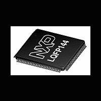
LPC2926_27_29 NXP Semiconductors, LPC2926_27_29 Datasheet - Page 72

LPC2926_27_29
Manufacturer Part Number
LPC2926_27_29
Description
The LPC2926/2927/2929 combine an ARM968E-S CPU core with two integrated TCMblocks operating at frequencies of up to 125 MHz, Full-speed USB 2
Manufacturer
NXP Semiconductors
Datasheet
1.LPC2926_27_29.pdf
(95 pages)
- Current page: 72 of 95
- Download datasheet (2Mb)
NXP Semiconductors
9. Dynamic characteristics
Table 36.
V
ground; positive currents flow into the IC; unless otherwise specified.
[1]
[2]
[3]
[4]
LPC2926_27_29
Product data sheet
Symbol
I/O pins
t
t
CLK_OUT pin
f
Internal clock
f
T
Low-power ring oscillator
f
t
Oscillator
f
t
PLL
f
f
t
t
Jitter specification for CAN
t
THL
TLH
clk
clk(sys)
ref(RO)
startup
i(osc)
startup
i(PLL)
o(PLL)
a(clk)
a(A)
jit(cc)(p-p)
DD(CORE)
clk(sys)
All parameters are guaranteed over the virtual junction temperature range by design. Pre-testing is performed at T
temperature on wafer level. Cased products are tested at T
test conditions to cover the specified temperature and power supply voltage range.
See
This parameter is not part of production testing or final testing, hence only a typical value is stated.
Oscillator start-up time depends on the quality of the crystal. For most crystals it takes about 1000 clock pulses until the clock is fully
stable.
Table
= V
Dynamic characteristics
DD(OSC_PLL)
27.
9.1 Dynamic characteristics: I/O and CLK_OUT pins, internal clock,
Parameter
HIGH to LOW transition
time
LOW to HIGH transition
time
clock frequency
system clock frequency
system clock period
RO reference
frequency
start-up time
oscillator input
frequency
start-up time
PLL input frequency
PLL output frequency
clock access time
address access time
cycle to cycle jitter
(peak-to-peak value)
oscillators, PLL, and CAN
; V
DD(IO)
= 2.7 V to 3.6 V; V
All information provided in this document is subject to legal disclaimers.
Conditions
C
C
on pin CLK_OUT
at maximum frequency
maximum frequency is
the clock input of an
external clock source
applied to the XIN_OSC
pin
at maximum frequency
CCO; direct mode
on CAN TXDC pin
L
L
Rev. 5 — 28 September 2010
= 30 pF
= 30 pF
DDA(ADC3V3)
amb
= 25 °C (final testing). Both pre-testing and final testing use correlated
= 3.0 V to 3.6 V; all voltages are measured with respect to
[1]
ARM9 microcontroller with CAN, LIN, and USB
[2]
[2]
[3]
[3]
[4]
[3]
Min
4
4
-
10
8
0.4
-
10
-
10
10
156
-
-
-
LPC2926/2927/2929
Typ
-
-
-
-
-
0.5
6
-
500
-
-
-
-
-
0.4
Max
13.8
13.8
40
125
100
0.6
-
100
-
25
160
320
63.4
60.3
1
© NXP B.V. 2010. All rights reserved.
amb
= 85 °C ambient
Unit
ns
ns
MHz
MHz
ns
MHz
μs
MHz
μs
MHz
MHz
MHz
ns
ns
ns
72 of 95
Related parts for LPC2926_27_29
Image
Part Number
Description
Manufacturer
Datasheet
Request
R
Part Number:
Description:
Lpc2926/2927/2929 Arm9 Microcontroller With Can, Lin, And Usb
Manufacturer:
NXP Semiconductors
Datasheet:
Part Number:
Description:
NXP Semiconductors designed the LPC2420/2460 microcontroller around a 16-bit/32-bitARM7TDMI-S CPU core with real-time debug interfaces that include both JTAG andembedded trace
Manufacturer:
NXP Semiconductors
Datasheet:

Part Number:
Description:
NXP Semiconductors designed the LPC2458 microcontroller around a 16-bit/32-bitARM7TDMI-S CPU core with real-time debug interfaces that include both JTAG andembedded trace
Manufacturer:
NXP Semiconductors
Datasheet:
Part Number:
Description:
NXP Semiconductors designed the LPC2468 microcontroller around a 16-bit/32-bitARM7TDMI-S CPU core with real-time debug interfaces that include both JTAG andembedded trace
Manufacturer:
NXP Semiconductors
Datasheet:
Part Number:
Description:
NXP Semiconductors designed the LPC2470 microcontroller, powered by theARM7TDMI-S core, to be a highly integrated microcontroller for a wide range ofapplications that require advanced communications and high quality graphic displays
Manufacturer:
NXP Semiconductors
Datasheet:
Part Number:
Description:
NXP Semiconductors designed the LPC2478 microcontroller, powered by theARM7TDMI-S core, to be a highly integrated microcontroller for a wide range ofapplications that require advanced communications and high quality graphic displays
Manufacturer:
NXP Semiconductors
Datasheet:
Part Number:
Description:
The Philips Semiconductors XA (eXtended Architecture) family of 16-bit single-chip microcontrollers is powerful enough to easily handle the requirements of high performance embedded applications, yet inexpensive enough to compete in the market for hi
Manufacturer:
NXP Semiconductors
Datasheet:
Part Number:
Description:
The XA-S3 device is a member of Philips Semiconductors? XA(eXtended Architecture) family of high performance 16-bitsingle-chip microcontrollers
Manufacturer:
NXP Semiconductors
Datasheet:

Part Number:
Description:
The NXP BlueStreak LH75401/LH75411 family consists of two low-cost 16/32-bit System-on-Chip (SoC) devices
Manufacturer:
NXP Semiconductors
Datasheet:

Part Number:
Description:
The NXP LPC3130/3131 combine an 180 MHz ARM926EJ-S CPU core, high-speed USB2
Manufacturer:
NXP Semiconductors
Datasheet:

Part Number:
Description:
The NXP LPC3141 combine a 270 MHz ARM926EJ-S CPU core, High-speed USB 2
Manufacturer:
NXP Semiconductors

Part Number:
Description:
The NXP LPC3143 combine a 270 MHz ARM926EJ-S CPU core, High-speed USB 2
Manufacturer:
NXP Semiconductors

Part Number:
Description:
The NXP LPC3152 combines an 180 MHz ARM926EJ-S CPU core, High-speed USB 2
Manufacturer:
NXP Semiconductors

Part Number:
Description:
The NXP LPC3154 combines an 180 MHz ARM926EJ-S CPU core, High-speed USB 2
Manufacturer:
NXP Semiconductors


