PCM18XK1 Microchip Technology, PCM18XK1 Datasheet - Page 103
PCM18XK1
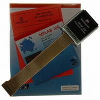
Manufacturer Part Number
PCM18XK1
Description
MODULE PROC PIC18F8680,6680,8565
Manufacturer
Microchip Technology
Datasheet
1.PCM18XK1.pdf
(496 pages)
Specifications of PCM18XK1
Accessory Type
Processor Module
Lead Free Status / RoHS Status
Not applicable / Not applicable
For Use With/related Products
ICE2000
For Use With
ICE2000 - EMULATOR MPLAB-ICE 2000 POD
Lead Free Status / Rohs Status
Lead free / RoHS Compliant


7.0
The data EEPROM is readable and writable during nor-
mal operation over the entire V
memory is not directly mapped in the register file
space. Instead, it is indirectly addressed through the
Special Function Registers (SFR).
There are five SFRs used to read and write the
program and data EEPROM memory. These registers
are:
• EECON1
• EECON2
• EEDATA
• EEADR
• EEADRH
The EEPROM data memory allows byte read and write.
When interfacing to the data memory block, EEDATA
holds the 8-bit data for read/write and EEADR holds the
address of the EEPROM location being accessed.
These devices have 1024 bytes of data EEPROM with
an address range from 0h to 3FFh.
The EEPROM data memory is rated for high erase/
write cycles. A byte write automatically erases the loca-
tion and writes the new data (erase-before-write). The
write time is controlled by an on-chip timer. The write
time will vary with voltage and temperature as well as
from chip to chip. Please refer to parameter D122
(Electrical Characteristics, Section 27.0 “Electrical
Characteristics”) for exact limits.
2004 Microchip Technology Inc.
DATA EEPROM MEMORY
DD
range. The data
PIC18F6585/8585/6680/8680
7.1
The address register pair, EEADRH:EEADR, can
address up to a maximum of 1024 bytes of data
EEPROM.
7.2
EECON1 is the control register for EEPROM memory
accesses.
EECON2 is not a physical register. Reading EECON2
will read all ‘0’s. The EECON2 register is used
exclusively in the EEPROM write sequence.
Control bits RD and WR initiate read and write opera-
tions, respectively. These bits cannot be cleared, only
set in software. They are cleared in hardware at the
completion of the read or write operation. The inability
to clear the WR bit in software prevents the accidental
or premature termination of a write operation.
The WREN bit, when set, will allow a write operation.
On power-up, the WREN bit is clear. The WRERR bit is
set when a write operation is interrupted by a MCLR
Reset or a WDT Time-out Reset during normal opera-
tion. In these situations, the user can check the
WRERR bit and rewrite the location. It is necessary to
reload the data and address registers (EEDATA and
EEADR) due to the Reset condition forcing the
contents of the registers to zero.
Note:
EECON1 and EECON2 Registers
EEADRH:EEADR
Interrupt flag bit, EEIF in the PIR2 register,
is set when write is complete. It must be
cleared in software.
DS30491C-page 101
Related parts for PCM18XK1
Image
Part Number
Description
Manufacturer
Datasheet
Request
R

Part Number:
Description:
Manufacturer:
Microchip Technology Inc.
Datasheet:
Part Number:
Description:
Manufacturer:
Microchip Technology Inc.
Datasheet:
Part Number:
Description:
Manufacturer:
Microchip Technology Inc.
Datasheet:
Part Number:
Description:
Manufacturer:
Microchip Technology Inc.
Datasheet:
Part Number:
Description:
Manufacturer:
Microchip Technology Inc.
Datasheet:
Part Number:
Description:
Manufacturer:
Microchip Technology Inc.
Datasheet:
Part Number:
Description:
Manufacturer:
Microchip Technology Inc.
Datasheet:
Part Number:
Description:
Manufacturer:
Microchip Technology Inc.
Datasheet: