PCM18XK1 Microchip Technology, PCM18XK1 Datasheet - Page 144
PCM18XK1
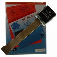
Manufacturer Part Number
PCM18XK1
Description
MODULE PROC PIC18F8680,6680,8565
Manufacturer
Microchip Technology
Datasheet
1.PCM18XK1.pdf
(496 pages)
Specifications of PCM18XK1
Accessory Type
Processor Module
Lead Free Status / RoHS Status
Not applicable / Not applicable
For Use With/related Products
ICE2000
For Use With
ICE2000 - EMULATOR MPLAB-ICE 2000 POD
Lead Free Status / Rohs Status
Lead free / RoHS Compliant


PIC18F6585/8585/6680/8680
10.7
PORTG is a 6-bit wide port with 5 bidirectional pins and
1 unidirectional pin. The corresponding data direction
register is TRISG. Setting a TRISG bit (= 1) will make
the corresponding PORTG pin an input (i.e., put the
corresponding output driver in a high-impedance
mode). Clearing a TRISG bit (= 0) will make the corre-
sponding PORTG pin an output (i.e., put the contents
of the output latch on the selected pin).
The Data Latch register (LATG) is also memory mapped.
Read-modify-write operations on the LATG register read
and write the latched output value for PORTG.
Pins RG0-RG2 on PORTG are multiplexed with the CAN
peripheral. Refer to Section 23.0 “ECAN Module” for
proper settings of TRISG when CAN is enabled. RG5 is
multiplexed with MCLR/V
more information.
When enabling peripheral functions, care should be
taken in defining TRIS bits for each PORTG pin. Some
peripherals override the TRIS bit to make a pin an output,
while other peripherals override the TRIS bit to make a
pin an input. The user should refer to the corresponding
peripheral section for the correct TRIS bit settings.
FIGURE 10-16:
DS30491C-page 142
Note:
Note: I/O pins have diode protection to V
Data Bus
WR PORTG or
WR LATG
WR TRISG
RD TRISG
RD PORTG
TXD
PORTG, TRISG and LATG
Registers
On a Power-on Reset, these pins are
configured as digital inputs.
RG0/CANTX1 PIN BLOCK DIAGRAM
PP
. Refer to Register 24-5 for
TRIS Latch
Data Latch
RD LATG
D
D
CK
CK
Q
Q
Q
Q
DD
and V
SS
0
1
OPMODE2:OPMODE0 = 000
.
The pin override value is not loaded into the TRIS reg-
ister. This allows read-modify-write of the TRIS register
without concern due to peripheral overrides.
EXAMPLE 10-7:
CLRF
CLRF
MOVLW 04h
MOVWF TRISG
Note 1: On a Power-on Reset, RG5 is enabled as
Q
EN
2: If the device Master Clear is disabled,
PORTG
LATG
EN
D
a digital input only if Master Clear
functionality is disabled (MCLRE = 0).
verify that either of the following is done to
ensure proper entry into ICSP mode:
a) disable Low-Voltage Programming
b) make certain that RB5/KBI1/PGM is
(CONFIG4L<2> = 0); or
held low during entry into ICSP.
V
V
P
N
DD
SS
; Initialize PORTG by
; clearing output
; data latches
; Alternate method
; to clear output
; data latches
; Value used to
; initialize data
; direction
; Set RG1:RG0 as outputs
; RG2 as input
; RG4:RG3 as inputs
ENDRHI
INITIALIZING PORT
OPMODE2:OPMODE0 = 000
2004 Microchip Technology Inc.
Schmitt
Trigger
I/O pin
Related parts for PCM18XK1
Image
Part Number
Description
Manufacturer
Datasheet
Request
R

Part Number:
Description:
Manufacturer:
Microchip Technology Inc.
Datasheet:
Part Number:
Description:
Manufacturer:
Microchip Technology Inc.
Datasheet:
Part Number:
Description:
Manufacturer:
Microchip Technology Inc.
Datasheet:
Part Number:
Description:
Manufacturer:
Microchip Technology Inc.
Datasheet:
Part Number:
Description:
Manufacturer:
Microchip Technology Inc.
Datasheet:
Part Number:
Description:
Manufacturer:
Microchip Technology Inc.
Datasheet:
Part Number:
Description:
Manufacturer:
Microchip Technology Inc.
Datasheet:
Part Number:
Description:
Manufacturer:
Microchip Technology Inc.
Datasheet: