PCM18XK1 Microchip Technology, PCM18XK1 Datasheet - Page 175
PCM18XK1
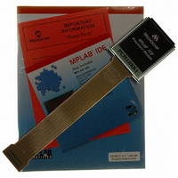
Manufacturer Part Number
PCM18XK1
Description
MODULE PROC PIC18F8680,6680,8565
Manufacturer
Microchip Technology
Datasheet
1.PCM18XK1.pdf
(496 pages)
Specifications of PCM18XK1
Accessory Type
Processor Module
Lead Free Status / RoHS Status
Not applicable / Not applicable
For Use With/related Products
ICE2000
For Use With
ICE2000 - EMULATOR MPLAB-ICE 2000 POD
Lead Free Status / Rohs Status
Lead free / RoHS Compliant


15.4
In Pulse Width Modulation (PWM) mode, the CCPx pin
produces up to a 10-bit resolution PWM output. For
PWM mode to function properly, the TRIS bit for the
CCPx pin must be cleared to make it an output.
Figure 15-3 shows a simplified block diagram of the
CCP module in PWM mode.
For a step-by-step procedure on how to set up the CCP
module for PWM operation, see Section 15.4.3
“Setup for PWM Operation”.
FIGURE 15-3:
A PWM output (Figure 15-4) has a time base (period)
and a time that the output stays high (duty cycle). The
frequency of the PWM is the inverse of the period
(1/period).
FIGURE 15-4:
2004 Microchip Technology Inc.
Note:
Note 1: 8-bit timer is concatenated with 2-bit internal Q clock or
CCPRxL (Master)
CCPRxH (Slave)
Comparator
TMR2 = PR2
Duty Cycle Registers
PR2
TMR2
PWM Mode
Comparator
2 bits of the prescaler to create 10-bit time base.
Duty Cycle
Clearing the CCPxCON register will force
the CCPx PWM output latch to the default
low level. This is not the port data latch.
Period
(Note 1)
TMR2 = Duty Cycle
Clear Timer,
set CCPx pin and
latch D.C.
SIMPLIFIED PWM BLOCK
DIAGRAM
PWM OUTPUT
TMR2 = PR2
CCPxCON<5:4>
R
S
Q
TRIS bit
PIC18F6585/8585/6680/8680
CCPx
15.4.1
The PWM period is specified by writing to the PR2
register. The PWM period can be calculated using the
following formula.
EQUATION 15-1:
PWM frequency is defined as 1/[PWM period].
When TMR2 is equal to PR2, the following three events
occur on the next increment cycle:
• TMR2 is cleared
• The CCP1 pin is set (exception: if PWM duty
• The PWM duty cycle is latched from CCPR1L into
15.4.2
The PWM duty cycle is specified by writing to the
CCPRxL register and to the CCPxCON<5:4> bits. Up
to 10-bit resolution is available. The CCPRxL contains
the eight MSbs and the CCPxCON<5:4> contain the
two LSbs. This 10-bit value is represented by
CCPRxL:CCPxCON<5:4>. The following equation is
used to calculate the PWM duty cycle in time.
EQUATION 15-2:
CCPRxL and CCPxCON<5:4> can be written to at any
time but the duty cycle value is not latched into
CCPRxH until after a match between PR2 and TMR2
occurs (i.e., the period is complete). In PWM mode,
CCPRxH is a read-only register.
The CCPRxH register and a 2-bit internal latch are
used to double-buffer the PWM duty cycle. This
double-buffering is essential for glitchless PWM
operation.
When the CCPRxH and 2-bit latch match TMR2,
concatenated with an internal 2-bit Q clock or 2 bits of
the TMR2 prescaler, the CCPx pin is cleared.
cycle = 0%, the CCP1 pin will not be set)
CCPR1H
Note:
PWM Duty Cycle = (CCPRxL:CCPxCON<5:4>) •
PWM Period = [(PR2) + 1] • 4 • T
PWM PERIOD
The Timer2 postscaler (see Section 13.0
“Timer2 Module”) is not used in the
determination of the PWM frequency. The
postscaler could be used to have a servo
update rate at a different frequency than
the PWM output.
PWM DUTY CYCLE
T
(TMR2 Prescale Value)
OSC
• (TMR2 Prescale Value)
DS30491C-page 173
OSC
•
Related parts for PCM18XK1
Image
Part Number
Description
Manufacturer
Datasheet
Request
R

Part Number:
Description:
Manufacturer:
Microchip Technology Inc.
Datasheet:
Part Number:
Description:
Manufacturer:
Microchip Technology Inc.
Datasheet:
Part Number:
Description:
Manufacturer:
Microchip Technology Inc.
Datasheet:
Part Number:
Description:
Manufacturer:
Microchip Technology Inc.
Datasheet:
Part Number:
Description:
Manufacturer:
Microchip Technology Inc.
Datasheet:
Part Number:
Description:
Manufacturer:
Microchip Technology Inc.
Datasheet:
Part Number:
Description:
Manufacturer:
Microchip Technology Inc.
Datasheet:
Part Number:
Description:
Manufacturer:
Microchip Technology Inc.
Datasheet: