PCM18XK1 Microchip Technology, PCM18XK1 Datasheet - Page 126
PCM18XK1
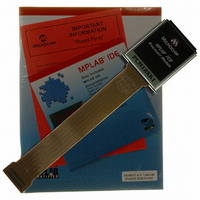
Manufacturer Part Number
PCM18XK1
Description
MODULE PROC PIC18F8680,6680,8565
Manufacturer
Microchip Technology
Datasheet
1.PCM18XK1.pdf
(496 pages)
Specifications of PCM18XK1
Accessory Type
Processor Module
Lead Free Status / RoHS Status
Not applicable / Not applicable
For Use With/related Products
ICE2000
For Use With
ICE2000 - EMULATOR MPLAB-ICE 2000 POD
Lead Free Status / Rohs Status
Lead free / RoHS Compliant


PIC18F6585/8585/6680/8680
9.6
External interrupts on the RB0/INT0, RB1/INT1, RB2/
INT2 and RB3/INT3 pins are edge-triggered: either ris-
ing if the corresponding INTEDGx bit is set in the
INTCON2 register, or falling if the INTEDGx bit is clear.
When a valid edge appears on the RBx/INTx pin, the
corresponding flag bit, INTxF, is set. This interrupt can
be disabled by clearing the corresponding enable bit,
INTxE. Flag bit, INTxF, must be cleared in software in
the Interrupt Service Routine before re-enabling the
interrupt. All external interrupts (INT0, INT1, INT2 and
INT3) can wake-up the processor from Sleep if bit
INTxIE was set prior to going into Sleep. If the global
interrupt enable bit GIE is set, the processor will branch
to the interrupt vector following wake-up.
The interrupt priority for INT, INT2 and INT3 is deter-
mined by the value contained in the interrupt priority
bits: INT1IP (INTCON3<6>), INT2IP (INTCON3<7>)
and INT3IP (INTCON2<1>). There is no priority bit
associated with INT0; it is always a high priority
interrupt source.
EXAMPLE 9-1:
DS30491C-page 124
MOVWF
MOVFF
MOVFF
;
; USER ISR CODE
;
MOVFF
MOVF
MOVFF
INT0 Interrupt
W_TEMP
STATUS, STATUS_TEMP
BSR, BSR_TEMP
BSR_TEMP, BSR
W_TEMP, W
STATUS_TEMP, STATUS
SAVING STATUS, WREG AND BSR REGISTERS IN RAM
; W_TEMP is in virtual bank
; STATUS_TEMP located anywhere
; BSR located anywhere
; Restore BSR
; Restore WREG
; Restore STATUS
9.7
In 8-bit mode (which is the default), an overflow in the
TMR0 register (0FFh
16-bit mode, an overflow in the TMR0H:TMR0L regis-
ters (0FFFFh
interrupt can be enabled/disabled by setting/clearing
enable bit, TMR0IE (INTCON<5>). Interrupt priority for
Timer0 is determined by the value contained in the
interrupt priority bit, TMR0IP (INTCON2<2>). See
Section 11.0 “Timer0 Module” for further details on
the Timer0 module.
9.8
An input change on PORTB<7:4> sets flag bit RBIF
(INTCON<0>). The interrupt can be enabled/disabled
by setting/clearing enable bit, RBIE (INTCON<3>).
Interrupt priority for PORTB interrupt-on-change is
determined by the value contained in the interrupt
priority bit, RBIP (INTCON2<0>).
9.9
During an interrupt, the return PC value is saved on the
stack. Additionally, the WREG, Status and BSR registers
are saved on the fast return stack. If a fast return from
interrupt is not used (See Section 4.3 “Fast Register
Stack”), the user may need to save the WREG, Status
and BSR registers in software. Depending on the user’s
application, other registers may also need to be saved.
Example 9-1 saves and restores the WREG, Status and
BSR registers during an Interrupt Service Routine.
TMR0 Interrupt
PORTB Interrupt-on-Change
Context Saving During Interrupts
0000h) will set flag bit, TMR0IF. The
2004 Microchip Technology Inc.
00h) will set flag bit TMR0IF. In
Related parts for PCM18XK1
Image
Part Number
Description
Manufacturer
Datasheet
Request
R

Part Number:
Description:
Manufacturer:
Microchip Technology Inc.
Datasheet:
Part Number:
Description:
Manufacturer:
Microchip Technology Inc.
Datasheet:
Part Number:
Description:
Manufacturer:
Microchip Technology Inc.
Datasheet:
Part Number:
Description:
Manufacturer:
Microchip Technology Inc.
Datasheet:
Part Number:
Description:
Manufacturer:
Microchip Technology Inc.
Datasheet:
Part Number:
Description:
Manufacturer:
Microchip Technology Inc.
Datasheet:
Part Number:
Description:
Manufacturer:
Microchip Technology Inc.
Datasheet:
Part Number:
Description:
Manufacturer:
Microchip Technology Inc.
Datasheet: