PCM18XK1 Microchip Technology, PCM18XK1 Datasheet - Page 90
PCM18XK1
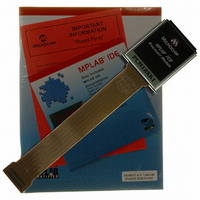
Manufacturer Part Number
PCM18XK1
Description
MODULE PROC PIC18F8680,6680,8565
Manufacturer
Microchip Technology
Datasheet
1.PCM18XK1.pdf
(496 pages)
Specifications of PCM18XK1
Accessory Type
Processor Module
Lead Free Status / RoHS Status
Not applicable / Not applicable
For Use With/related Products
ICE2000
For Use With
ICE2000 - EMULATOR MPLAB-ICE 2000 POD
Lead Free Status / Rohs Status
Lead free / RoHS Compliant


PIC18F6585/8585/6680/8680
5.4
The minimum erase block is 32 words or 64 bytes. Only
through the use of an external programmer or through
ICSP control can larger blocks of program memory be
bulk erased. Word erase in the Flash array is not
supported.
When initiating an erase sequence from the micro-
controller itself, a block of 64 bytes of program memory
is erased. The Most Significant 16 bits of the
TBLPTR<21:6> point to the block being erased.
TBLPTR<5:0> are ignored.
The EECON1 register commands the erase operation.
The EEPGD bit must be set to point to the Flash
program memory. The WREN bit must be set to enable
write operations. The FREE bit is set to select an erase
operation.
For protection, the write initiate sequence for EECON2
must be used.
A long write is necessary for erasing the internal Flash.
Instruction execution is halted while in a long write
cycle. The long write will be terminated by the internal
programming timer.
EXAMPLE 5-2:
DS30491C-page 88
Required
Sequence
Erasing Flash Program Memory
ERASE_ROW
ERASING A FLASH PROGRAM MEMORY ROW
MOVLW
MOVWF
MOVLW
MOVWF
MOVLW
MOVWF
BSF
BCF
BSF
BSF
BCF
MOVLW
MOVWF
MOVLW
MOVWF
BSF
NOP
BSF
upper(CODE_ADDR)
TBLPTRU
high(CODE_ADDR)
TBLPTRH
low(CODE_ADDR)
TBLPTRL
EECON1, EEPGD
EECON1, CFGS
EECON1, WREN
EECON1, FREE
INTCON, GIE
55h
EECON2
0AAh
EECON2
EECON1, WR
INTCON, GIE
; load TBLPTR with the base
; address of the memory block
; point to Flash program memory
; access Flash program memory
; enable write to memory
; enable Row Erase operation
; disable interrupts
; write 55h
; write 0AAh
; start erase (CPU stall)
; re-enable interrupts
5.4.1
The sequence of events for erasing a block of internal
program memory location is:
1.
2.
3.
4.
5.
6.
7.
8.
9.
Load table pointer with address of row being
erased.
Set the EECON1 register for the erase
operation:
• set EEPGD bit to point to program memory;
• clear the CFGS bit to access program memory;
• set WREN bit to enable writes;
• set FREE bit to enable the erase.
Disable interrupts.
Write 55h to EECON2.
Write 0AAh to EECON2.
Set the WR bit. This will begin the row erase
cycle.
The CPU will stall for duration of the erase
(about 2 ms using internal timer).
Execute a NOP.
Re-enable interrupts.
FLASH PROGRAM MEMORY
ERASE SEQUENCE
2004 Microchip Technology Inc.
Related parts for PCM18XK1
Image
Part Number
Description
Manufacturer
Datasheet
Request
R

Part Number:
Description:
Manufacturer:
Microchip Technology Inc.
Datasheet:
Part Number:
Description:
Manufacturer:
Microchip Technology Inc.
Datasheet:
Part Number:
Description:
Manufacturer:
Microchip Technology Inc.
Datasheet:
Part Number:
Description:
Manufacturer:
Microchip Technology Inc.
Datasheet:
Part Number:
Description:
Manufacturer:
Microchip Technology Inc.
Datasheet:
Part Number:
Description:
Manufacturer:
Microchip Technology Inc.
Datasheet:
Part Number:
Description:
Manufacturer:
Microchip Technology Inc.
Datasheet:
Part Number:
Description:
Manufacturer:
Microchip Technology Inc.
Datasheet: