PCM18XK1 Microchip Technology, PCM18XK1 Datasheet - Page 449
PCM18XK1
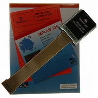
Manufacturer Part Number
PCM18XK1
Description
MODULE PROC PIC18F8680,6680,8565
Manufacturer
Microchip Technology
Datasheet
1.PCM18XK1.pdf
(496 pages)
Specifications of PCM18XK1
Accessory Type
Processor Module
Lead Free Status / RoHS Status
Not applicable / Not applicable
For Use With/related Products
ICE2000
For Use With
ICE2000 - EMULATOR MPLAB-ICE 2000 POD
Lead Free Status / Rohs Status
Lead free / RoHS Compliant


FIGURE 27-25:
TABLE 27-26: A/D CONVERSION REQUIREMENTS
2004 Microchip Technology Inc.
130
131
132
135
136
Note 1:
Param.
No.
Note 1: If the A/D clock source is selected as RC, a time of T
2:
3:
4:
5:
A/D DATA
SAMPLE
A/D CLK
ADRES
2: This is a minimal RC delay (typically 100 ns) which also disconnects the holding capacitor from the analog input.
T
T
T
T
T
Symbol
BSF ADCON0, GO
AD
CNV
ACQ
SWC
AMP
ADIF
ADRES register may be read on the following T
See Section 19.0 “10-bit Analog-to-Digital Converter (A/D) Module” for minimum conditions when input
voltage has changed more than 1 LSb.
The time for the holding capacitor to acquire the “New” input voltage when the voltage changes full scale
after the conversion (AV
50 .
On the next Q4 cycle of the device clock.
The time of the A/D clock period is dependent on the device frequency and the T
executed.
GO
Q4
132
A/D Clock Period
Conversion Time
(not including acquisition time) (Note 1)
Acquisition Time (Note 3)
Switching Time from Convert
Amplifier Settling Time (Note 2)
A/D CONVERSION TIMING
(Note 2)
Characteristic
DD
9
to AV
PIC18FXX8X
PIC18LFXX8X
PIC18FXX8X
PIC18LFXX8X
8
SS
PIC18F6585/8585/6680/8680
, or AV
OLD_DATA
7
Sample
CY
SS
is added before the A/D clock starts. This allows the SLEEP instruction to be
. . .
SAMPLING STOPPED
to AV
CY
DD
cycle.
. . .
131
130
). The source impedance (R
Min
1.6
3.0
2.0
3.0
11
15
10
—
1
2
(Note 4)
20
20
Max
6.0
9.0
12
—
—
—
(5)
(5)
1
Units
T
AD
s
s
s
s
s
s
s
0
T
T
A/D RC mode
A/D RC mode
-40 C
0 C
This may be used if the
“new” input voltage has not
changed by more than 1 LSb
(i.e., 5 mV @ 5.12V) from the
last sampled voltage (as
stated on C
OSC
OSC
AD
S
) on the input channels is
clock divider.
based, V
based, V
Temp
NEW_DATA
DONE
Temp
Conditions
DS30491C-page 447
HOLD
T
CY
+125 C
REF
REF
+125 C
).
full range
3.0V
Related parts for PCM18XK1
Image
Part Number
Description
Manufacturer
Datasheet
Request
R

Part Number:
Description:
Manufacturer:
Microchip Technology Inc.
Datasheet:
Part Number:
Description:
Manufacturer:
Microchip Technology Inc.
Datasheet:
Part Number:
Description:
Manufacturer:
Microchip Technology Inc.
Datasheet:
Part Number:
Description:
Manufacturer:
Microchip Technology Inc.
Datasheet:
Part Number:
Description:
Manufacturer:
Microchip Technology Inc.
Datasheet:
Part Number:
Description:
Manufacturer:
Microchip Technology Inc.
Datasheet:
Part Number:
Description:
Manufacturer:
Microchip Technology Inc.
Datasheet:
Part Number:
Description:
Manufacturer:
Microchip Technology Inc.
Datasheet: