EVAL-ADT7411EBZ Analog Devices Inc, EVAL-ADT7411EBZ Datasheet - Page 15
EVAL-ADT7411EBZ
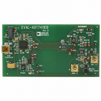
Manufacturer Part Number
EVAL-ADT7411EBZ
Description
BOARD EVALUATION FOR ADT7411
Manufacturer
Analog Devices Inc
Datasheet
1.ADT7411ARQZ.pdf
(36 pages)
Specifications of EVAL-ADT7411EBZ
Sensor Type
Temperature
Sensing Range
-40°C ~ 120°C
Interface
DSP, I²C, MICROWIRE, QSPI, SMBus, SPI
Sensitivity
±0.5°C
Voltage - Supply
2.7 V ~ 5.5 V
Embedded
No
Utilized Ic / Part
ADT7411
Lead Free Status / RoHS Status
Lead free / RoHS Compliant


ADC Transfer Function
The output coding of the ADT7411 analog inputs is straight
binary. The designed code transitions occur midway between
successive integer LSB values (that is, 1/2 LSB, 3/2 LSB). The
LSB is V
transfer characteristic is shown in Figure 24.
To work out the voltage on any analog input channel, the
following method is used.
Convert the value read back from the AIN value register into
decimal.
where d is the decimal.
Example:
Internal reference used. Therefore, V
AIN Value = 512d
1 LSB Size = 2.25 V/1024 = 2.197 × 10
AIN Voltage = 512 × 2.197 × 10
Analog Input ESD Protection
Figure 26 shows the input structure that provides ESD protec-
tion on any of the analog input pins. The diode provides the
main ESD protection for the analog inputs. Care must be taken
that the analog input signal never drops below the GND rail by
more than 200 mV. If this happens, the diode becomes forward
biased and starts conducting current into the substrate. The
4 pF capacitor is the typical pin capacitance and the resistor is a
lumped component made up of the on resistance of the
multiplexer switch.
1 LSB = Reference (V)/1024
AIN Voltage = AIN Value (d) × LSB Size
DD
/1024 or Int V
111...111
111...110
111...000
011...111
000...010
000...001
000...000
= 1.125 V
0V 1/2 LSB
Figure 24. Transfer Function
REF
/1024, Int V
ANALOG INPUT
−3
1LSB = INT V
1LSB = V
+V
REF
REF
−3
REF
DD
= 2.25 V.
– 1LSB
/1024
= 2.25 V. The ideal
REF
/1024
Rev. B | Page 15 of 36
AIN Interrupts
The measured results from the AIN inputs are compared with
the AIN V
equal to comparison) limits. An interrupt occurs if the AIN
inputs exceed or equal the limit registers. These voltage limits
are stored in on-chip registers. Note that the limit registers are
eight bits long while the AIN conversion result is 10 bits long.
If the voltage limits are not masked out, any out-of-limit
comparisons generate flags that are stored in the Interrupt
Status 1 register (Address 00h) and one or more out-of-limit
results will cause the INT/ INT output to pull either high or
low, depending on the output polarity setting. It is good design
practice to mask out interrupts for channels that are of no
concern to the application. Figure 27 shows the interrupt
structure for the ADT7411. It shows a block diagram
representation of how the various measurement channels
affect the INT/ INT pin.
FUNCTIONAL DESCRIPTION—MEASUREMENT
Temperature Sensor
The ADT7411 contains an ADC with special input signal
conditioning to enable operation with external and on-chip
diode temperature sensors. When the ADT7411 is operating in
single-channel mode, the ADC continually processes the
measurement taken on one channel only. This channel is
preselected by Bit C0 to Bit C3 in the Control Configuration 2
register (Address 19h). When in round robin mode, the analog
input multiplexer sequentially selects the V
on-chip temperature sensor to measure its internal temperature,
the external temperature sensor, or an AIN channel, and then
the rest of the AIN channels. These signals are digitized by the
ADC and the results stored in the various value registers.
INTERNAL
SENSE
TRANSISTOR
Figure 25. Top Level Structure of Internal Temperature Sensor
I
HIGH
Figure 26. Equivalent Analog Input ESD Circuit
(greater than comparison) and V
N × I
AIN
BIAS
DIODE
4pF
I
BIAS
V
DD
100Ω
DD
input channel,
LOW
ADT7411
(less than or
TO ADC
V
V
OUT+
OUT–
Related parts for EVAL-ADT7411EBZ
Image
Part Number
Description
Manufacturer
Datasheet
Request
R


Part Number:
Description:
BOARD EVAL FOR SI270X-A
Manufacturer:
Silicon Laboratories Inc
Datasheet:

Part Number:
Description:
BUCK CONV REF DESIGN KIT IP1201
Manufacturer:
International Rectifier
Datasheet:
Part Number:
Description:
BOARD DEMO SYNC DUAL BUCK CNVTER
Manufacturer:
International Rectifier
Datasheet:
Part Number:
Description:
BOARD DEMO SYNC BUCK CONVETER
Manufacturer:
International Rectifier
Datasheet:

Part Number:
Description:
EVALBOARD/EB Omnidirectional microphone - Analog
Manufacturer:
Analog Devices
Datasheet:
Part Number:
Description:
EVALBOARD/EB Omnidirectional microphone - Analog
Manufacturer:
Analog Devices
Datasheet:


Part Number:
Description:
BOARD EVAL LED DRIVER LT3756
Manufacturer:
Linear Technology
Datasheet:

Part Number:
Description:
BOARD EVAL FOR AD7741/7742
Manufacturer:
Analog Devices Inc
Datasheet:

Part Number:
Description:
±1.7g Dual-Axis IMEMS Accelerometer Evaluation Board
Manufacturer:
Analog Devices Inc
Datasheet:

Part Number:
Description:
IC MULTIPLIER ANALOG 8-SOIC T/R
Manufacturer:
Analog Devices Inc
Datasheet:

Part Number:
Description:
IC ANALOG MULTIPLIER 8-DIP
Manufacturer:
Analog Devices Inc
Datasheet:
Part Number:
Description:
IC ANALOG MULTIPLIER 8-SOIC
Manufacturer:
Analog Devices Inc
Datasheet:
Part Number:
Description:
IC ANALOG MULTIPLIER 8-DIP
Manufacturer:
Analog Devices Inc
Datasheet: