EVAL-ADT7411EBZ Analog Devices Inc, EVAL-ADT7411EBZ Datasheet - Page 30
EVAL-ADT7411EBZ
Manufacturer Part Number
EVAL-ADT7411EBZ
Description
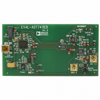
BOARD EVALUATION FOR ADT7411
Manufacturer
Analog Devices Inc
Datasheet
1.ADT7411ARQZ.pdf
(36 pages)
Specifications of EVAL-ADT7411EBZ
Sensor Type
Temperature
Sensing Range
-40°C ~ 120°C
Interface
DSP, I²C, MICROWIRE, QSPI, SMBus, SPI
Sensitivity
±0.5°C
Voltage - Supply
2.7 V ~ 5.5 V
Embedded
No
Utilized Ic / Part
ADT7411
Lead Free Status / RoHS Status
Lead free / RoHS Compliant


ADT7411
2.
3.
The peripheral whose address corresponds to the
transmitted address responds by pulling the data line low
during the low period before the ninth clock pulse, known
as the acknowledge bit. All other devices on the bus now
remain idle while the selected device waits for data to be
read from or written to it. If the R/ W bit is 0, the master
writes to the slave device. If the R/ W bit is 1, the master
reads from the slave device.
Data is sent over the serial bus in sequences of nine clock
pulses: eight bits of data followed by an acknowledge bit
from the receiver of data. Transitions on the data line must
occur during the low period of the clock signal and remain
stable during the high period because a low-to-high
transition when the clock is high can be interpreted as a
stop signal.
When all data bytes are read or written, stop conditions are
established. In write mode, the master pulls the data line
high during the 10th clock pulse to assert a stop condition.
In read mode, the master device pulls the data line high
during the low period before the ninth clock pulse. This is
known as No Acknowledge. The master then takes the data
line low during the low period before the 10th clock pulse,
and then high during the 10th clock pulse to assert a stop
condition.
Any number of bytes of data can be transferred over the
serial bus in one operation, but it is not possible to mix
read and write in one operation. This is because the type of
operation is determined at the beginning and cannot
subsequently be changed without starting a new operation.
The I
the device until after this address is sent twice. On the
eighth SCL cycle of the second valid communication, the
serial bus address is latched in. This is the SCL cycle
directly after the device has seen its own I
address. Any subsequent changes on this pin will have no
effect on the I
2
C address set up by the ADD pin is not latched by
2
C serial bus address.
2
C serial bus
Rev. B | Page 30 of 36
Writing to the ADT7411
Depending on the register being written to, there are two
different writes for the ADT7411. It is not possible to do a block
write to this part, that is, no I
Writing to the Address Pointer Register for a Subsequent
Read
To read data from a particular register, the address pointer
register must contain the address of that register. If it does not,
the correct address must be written to the address pointer
register by performing a single-byte write operation, as shown
in Figure 34. The write operation consists of the serial bus
address followed by the address pointer byte. No data is written
to any of the data registers. A read operation is then performed
to read the register.
Writing Data to a Register
All registers are 8-bit registers so only one byte of data can be
written to each register. Writing a single byte of data to one of
these read/write registers consists of the serial bus address, the
data register address written to the address pointer register,
followed by the data byte written to the selected data register
(see Figure 35). To write to a different register, another START
or repeated START is required. If more than one byte of data is
sent in one communication operation, the addressed register is
repeatedly loaded until the last data byte is sent.
Reading Data from the ADT7411
Reading data from the ADT7411 is done in a one-byte
operation. Reading back the contents of a register is shown in
Figure 36. The register address was previously set up by a
single-byte write operation to the Address Pointer register. To
read from another register, write to the Address Pointer register
again to set up the relevant register address. Therefore, block
reads are not possible, that is, no I
SPI Serial Interface
The SPI serial interface of the ADT7411 consists of four wires:
CS , SCLK, DIN, and DOUT. The CS is used to select the device
when more than one device is connected to the serial clock and
data lines. The CS is also used to distinguish between any two
separate serial communications (see Figure 41 for a graphical
explanation). The SCLK is used to clock data in and out of the
part. The DIN line is used to write to the registers, and the
DOUT line is used to read data back from the registers. The
recommended pull-up resistor value is between 500 Ω and
820 Ω. Strong pull-ups are needed when serial clock speeds that
are close to the maximum limit are used or when the SPI
interface lines are experiencing large capacitive loading. Larger
resistor values can be used for pull-up resistors when the serial
clock speed is reduced.
2
C auto-increment.
2
C auto-increment.
Related parts for EVAL-ADT7411EBZ
Image
Part Number
Description
Manufacturer
Datasheet
Request
R


Part Number:
Description:
BOARD EVAL FOR SI270X-A
Manufacturer:
Silicon Laboratories Inc
Datasheet:

Part Number:
Description:
BUCK CONV REF DESIGN KIT IP1201
Manufacturer:
International Rectifier
Datasheet:
Part Number:
Description:
BOARD DEMO SYNC DUAL BUCK CNVTER
Manufacturer:
International Rectifier
Datasheet:
Part Number:
Description:
BOARD DEMO SYNC BUCK CONVETER
Manufacturer:
International Rectifier
Datasheet:

Part Number:
Description:
EVALBOARD/EB Omnidirectional microphone - Analog
Manufacturer:
Analog Devices
Datasheet:
Part Number:
Description:
EVALBOARD/EB Omnidirectional microphone - Analog
Manufacturer:
Analog Devices
Datasheet:


Part Number:
Description:
BOARD EVAL LED DRIVER LT3756
Manufacturer:
Linear Technology
Datasheet:

Part Number:
Description:
BOARD EVAL FOR AD7741/7742
Manufacturer:
Analog Devices Inc
Datasheet:

Part Number:
Description:
±1.7g Dual-Axis IMEMS Accelerometer Evaluation Board
Manufacturer:
Analog Devices Inc
Datasheet:

Part Number:
Description:
IC MULTIPLIER ANALOG 8-SOIC T/R
Manufacturer:
Analog Devices Inc
Datasheet:

Part Number:
Description:
IC ANALOG MULTIPLIER 8-DIP
Manufacturer:
Analog Devices Inc
Datasheet:
Part Number:
Description:
IC ANALOG MULTIPLIER 8-SOIC
Manufacturer:
Analog Devices Inc
Datasheet:
Part Number:
Description:
IC ANALOG MULTIPLIER 8-DIP
Manufacturer:
Analog Devices Inc
Datasheet: