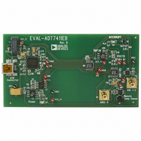
EVAL-ADT7411EBZ Analog Devices Inc, EVAL-ADT7411EBZ Datasheet - Page 4
EVAL-ADT7411EBZ
Manufacturer Part Number
EVAL-ADT7411EBZ
Description
BOARD EVALUATION FOR ADT7411
Manufacturer
Analog Devices Inc
Datasheet
1.ADT7411ARQZ.pdf
(36 pages)
Specifications of EVAL-ADT7411EBZ
Sensor Type
Temperature
Sensing Range
-40°C ~ 120°C
Interface
DSP, I²C, MICROWIRE, QSPI, SMBus, SPI
Sensitivity
±0.5°C
Voltage - Supply
2.7 V ~ 5.5 V
Embedded
No
Utilized Ic / Part
ADT7411
Lead Free Status / RoHS Status
Lead free / RoHS Compliant


ADT7411
Parameter
ROUND ROBIN UPDATE RATE
ON-CHIP REFERENCE
DIGITAL INPUTS
DIGITAL OUTPUTS
I
SPI TIMING CHARACTERISTICS
2
C TIMING CHARACTERISTICS
Slow ADC @ 25°C
Fast ADC @ 25°C
Reference Voltage
Temperature Coefficient
Input Current
V
V
Pin Capacitance
SCL, SDA Glitch Rejection
Output High Voltage, V
Output Low Voltage, V
Output High Current, I
Output Capacitance, C
INT/INT Output Saturation Voltage
Serial Clock Period, t
Data In Setup Time to SCL High, t
Data Out Stable after SCL Low, t
SDA Low Setup Time to SCL Low
SDA High Hold Time after SCL High
SDA and SCL Fall Time, t
SDA and SCL Rise Time, t
CS to SCLK Setup Time, t
SCLK High Pulse Width, t
SCLK Low Pulse Width, t
Data Access Time after SCLK Falling Edge, t
Data Setup Time Prior to SCLK Rising Edge, t
Data Hold Time after SCLK Rising Edge, t
CS to SCLK Hold Time, t
CS to DOUT High Impedance, t
IL
IH
, Input Low Voltage
Averaging On
Averaging Off
Averaging On
Averaging Off
Averaging On
Averaging Off
Averaging On
Averaging Off
(Start Condition), t
(Stop Condition), t
, Input High Voltage
1
1, 3
3
1
5
4
OL
OH
OUT
OH
7
3
6
1
7
2
2
4, 5
1, 3, 7
8
3
2
6
4
7
5
Min
2.2662
1.89
2.4
2.5
50
0
50
50
0
50
50
20
0
0
Typ
125.4
17.1
140.36
12.11
9.26
578.96
24.62
3.25
2.28
80
3
Rev. B | Page 4 of 36
Max
2.2938
±1
0.8
10
50
0.4
1
50
0.8
300
300
35
40
6
Unit
ms
ms
ms
ms
ms
μs
ms
ms
V
ppm/°C
μA
V
V
pF
ns
V
V
mA
pF
V
μs
ns
ns
ns
ns
ns
ns
ns
ns
ns
ns
ns
ns
ns
ns
Conditions/Comments
Time to complete one measurement cycle
through all channels.
AIN1 and AIN2 are selected on Pin 7 and Pin 8.
AIN1 and AIN2 are selected on Pin 7 and Pin 8.
D+ and D– are selected on Pin 7 and Pin 8.
D+ and D− are selected on Pin 7 and Pin 8.
AIN1 and AIN2 are selected on Pin 7 and Pin 8.
AIN1 and AIN2 are selected on Pin 7 and Pin 8.
D+ and D− are selected on Pin 7 and Pin 8.
D+ and D− are selected on Pin 7 and Pin 8.
V
All digital inputs.
Input filtering suppresses noise spikes of less
than 50 ns.
I
I
V
I
Fast-mode I
See Figure 2.
See Figure 2.
See Figure 2.
See Figure 2.
See Figure 2.
See Figure 3.
See Figure 3.
See Figure 3.
See Figure 3.
See Figure 3.
See Figure 3.
See Figure 3.
See Figure 3.
SOURCE
OL
OUT
IN
OH
= 3 mA.
= 0 V to V
= 5 V.
= 4 mA.
= I
SINK
2
= 200 μA.
C. See Figure 2.
DD
.
Related parts for EVAL-ADT7411EBZ
Image
Part Number
Description
Manufacturer
Datasheet
Request
R


Part Number:
Description:
BOARD EVAL FOR SI270X-A
Manufacturer:
Silicon Laboratories Inc
Datasheet:

Part Number:
Description:
BUCK CONV REF DESIGN KIT IP1201
Manufacturer:
International Rectifier
Datasheet:
Part Number:
Description:
BOARD DEMO SYNC DUAL BUCK CNVTER
Manufacturer:
International Rectifier
Datasheet:
Part Number:
Description:
BOARD DEMO SYNC BUCK CONVETER
Manufacturer:
International Rectifier
Datasheet:

Part Number:
Description:
EVALBOARD/EB Omnidirectional microphone - Analog
Manufacturer:
Analog Devices
Datasheet:
Part Number:
Description:
EVALBOARD/EB Omnidirectional microphone - Analog
Manufacturer:
Analog Devices
Datasheet:


Part Number:
Description:
BOARD EVAL LED DRIVER LT3756
Manufacturer:
Linear Technology
Datasheet:

Part Number:
Description:
BOARD EVAL FOR AD7741/7742
Manufacturer:
Analog Devices Inc
Datasheet:

Part Number:
Description:
±1.7g Dual-Axis IMEMS Accelerometer Evaluation Board
Manufacturer:
Analog Devices Inc
Datasheet:

Part Number:
Description:
IC MULTIPLIER ANALOG 8-SOIC T/R
Manufacturer:
Analog Devices Inc
Datasheet:

Part Number:
Description:
IC ANALOG MULTIPLIER 8-DIP
Manufacturer:
Analog Devices Inc
Datasheet:
Part Number:
Description:
IC ANALOG MULTIPLIER 8-SOIC
Manufacturer:
Analog Devices Inc
Datasheet:
Part Number:
Description:
IC ANALOG MULTIPLIER 8-DIP
Manufacturer:
Analog Devices Inc
Datasheet: