EVAL-ADT7411EBZ Analog Devices Inc, EVAL-ADT7411EBZ Datasheet - Page 27
EVAL-ADT7411EBZ
Manufacturer Part Number
EVAL-ADT7411EBZ
Description
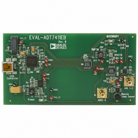
BOARD EVALUATION FOR ADT7411
Manufacturer
Analog Devices Inc
Datasheet
1.ADT7411ARQZ.pdf
(36 pages)
Specifications of EVAL-ADT7411EBZ
Sensor Type
Temperature
Sensing Range
-40°C ~ 120°C
Interface
DSP, I²C, MICROWIRE, QSPI, SMBus, SPI
Sensitivity
±0.5°C
Voltage - Supply
2.7 V ~ 5.5 V
Embedded
No
Utilized Ic / Part
ADT7411
Lead Free Status / RoHS Status
Lead free / RoHS Compliant


AIN2 V
This limit register is an 8-bit read/write register that stores the
AIN2 input lower limit that causes an interrupt and activates
the INT/ INT output (if enabled). For this to happen, the
measured AIN2 value has to be less than or equal to the value in
this register. Because it is an 8-bit register, the resolution is four
times less than the resolution of the 10-bit ADC. The default
value is 0 V.
Table 47. AIN2 V
D7
D7
0
1
AIN3 V
This limit register is an 8-bit read/write register that stores the
AIN3 input upper limit that causes an interrupt and activates
the INT/ INT output (if enabled). For this to happen, the
measured AIN3 value has to be greater than the value in this
register. Because it is an 8-bit register, the resolution is four
times less than the resolution of the 10-bit ADC. The default
value is full-scale voltage.
Table 48. AIN3 V
D7
D7
1
1
AIN3 V
This limit register is an 8-bit read/write register that stores the
AIN3 input lower limit that causes an interrupt and activates
the INT/ INT output (if enabled). For this to happen, the
measured AIN3 value has to be less than or equal to the value in
this register. Because it is an 8-bit register, the resolution is four
times less than the resolution of the 10-bit ADC. The default
value is 0 V.
Table 49. AIN3 V
D7
D7
0
1
AIN4 V
This limit register is an 8-bit read/write register that stores the
AIN4 input upper limit that causes an interrupt and activates
the INT/ INT output (if enabled). For this to happen, the
measured AIN4 value has to be greater than the value in this
register. Because it is an 8-bit register, the resolution is four
times less than the resolution of the 10-bit ADC. The default
value is full-scale voltage.
Default settings at power-up.
Default settings at power-up.
Default settings at power-up.
1
1
1
LOW
HIGH
LOW
HIGH
D6
D6
0
D6
D6
1
D6
D6
0
1
1
1
Limit Register (Read/Write) [Address = 2Ch]
Limit Register (Read/Write) [Address = 2Eh]
Limit Register (Read/Write) [Address = 2Fh]
Limit Register (Read/Write) [Address = 2Dh]
D5
D5
0
D5
D5
1
D5
D5
0
1
1
1
LOW
HIGH
LOW
Limit
Limit
Limit
D4
D4
0
D4
D4
1
D4
D4
0
1
1
1
D3
D3
0
D3
D3
1
D3
D3
0
1
1
1
D2
D2
0
D2
D2
1
D2
D2
0
1
1
1
D1
D1
0
D1
D1
1
D1
D1
0
1
1
1
D0
D0
0
D0
D0
1
D0
D0
0
1
1
1
Rev. B | Page 27 of 36
Table 50. AIN4 V
D7
D7
1
1
AIN4 V
This limit register is an 8-bit read/write register that stores the
AIN4 input lower limit that causes an interrupt and activates
the INT/ INT output (if enabled). For this to happen, the measured
AIN4 value has to be less than or equal to the value in this
register. Because it is an 8-bit register, the resolution is four
times less than the resolution of the 10-bit ADC. The default
value is 0 V.
Table 51. AIN4 V
D7
D7
0
1
AIN5 V
This limit register is an 8-bit read/write register that stores the
AIN5 input upper limit that causes an interrupt and activates
the INT/ INT output (if enabled). For this to happen, the
measured AIN5 value has to be greater than the value in this
register. Because it is an 8-bit register, the resolution is four
times less than the resolution of the 10-bit ADC. The default
value is full-scale voltage.
Table 52. AIN5 V
D7
D7
1
1
AIN5 V
This limit register is an 8-bit read/write register that stores the
AIN5 input lower limit that causes an interrupt and activates
the INT/ INT output (if enabled). For this to happen, the
measured AIN5 value has to be less than or equal to the value in
this register. Because it is an 8-bit register, the resolution is four
times less than the resolution of the 10-bit ADC. The default
value is 0 V.
Table 53. AIN5 V
D7
D7
0
1
Default settings at power-up.
Default settings at power-up.
Default settings at power-up.
Default settings at power-up.
1
1
1
1
LOW
HIGH
LOW
D6
D6
1
D6
D6
0
D6
D6
1
D6
D6
0
1
1
1
1
Limit Register (Read/Write) [Address = 30h]
Limit Register (Read/Write) [Address = 32h]
Limit Register (Read/Write) [Address = 31h]
D5
D5
1
D5
D5
0
D5
D5
1
D5
D5
0
1
1
1
1
HIGH
LOW
HIGH
LOW
Limit
Limit
Limit
Limit
D4
D4
1
D4
D4
0
D4
D4
1
D4
D4
0
1
1
1
1
D3
D3
1
D3
D3
0
D3
D3
1
D3
D3
0
1
1
1
1
D2
D2
1
D2
D2
0
D2
D2
1
D2
D2
0
1
1
1
1
ADT7411
D1
D1
1
D1
D1
0
D1
D1
1
D1
D1
0
1
1
1
1
D0
D0
1
D0
D0
0
D0
D0
1
D0
D0
0
1
1
1
1
Related parts for EVAL-ADT7411EBZ
Image
Part Number
Description
Manufacturer
Datasheet
Request
R


Part Number:
Description:
BOARD EVAL FOR SI270X-A
Manufacturer:
Silicon Laboratories Inc
Datasheet:

Part Number:
Description:
BUCK CONV REF DESIGN KIT IP1201
Manufacturer:
International Rectifier
Datasheet:
Part Number:
Description:
BOARD DEMO SYNC DUAL BUCK CNVTER
Manufacturer:
International Rectifier
Datasheet:
Part Number:
Description:
BOARD DEMO SYNC BUCK CONVETER
Manufacturer:
International Rectifier
Datasheet:

Part Number:
Description:
EVALBOARD/EB Omnidirectional microphone - Analog
Manufacturer:
Analog Devices
Datasheet:
Part Number:
Description:
EVALBOARD/EB Omnidirectional microphone - Analog
Manufacturer:
Analog Devices
Datasheet:


Part Number:
Description:
BOARD EVAL LED DRIVER LT3756
Manufacturer:
Linear Technology
Datasheet:

Part Number:
Description:
BOARD EVAL FOR AD7741/7742
Manufacturer:
Analog Devices Inc
Datasheet:

Part Number:
Description:
±1.7g Dual-Axis IMEMS Accelerometer Evaluation Board
Manufacturer:
Analog Devices Inc
Datasheet:

Part Number:
Description:
IC MULTIPLIER ANALOG 8-SOIC T/R
Manufacturer:
Analog Devices Inc
Datasheet:

Part Number:
Description:
IC ANALOG MULTIPLIER 8-DIP
Manufacturer:
Analog Devices Inc
Datasheet:
Part Number:
Description:
IC ANALOG MULTIPLIER 8-SOIC
Manufacturer:
Analog Devices Inc
Datasheet:
Part Number:
Description:
IC ANALOG MULTIPLIER 8-DIP
Manufacturer:
Analog Devices Inc
Datasheet: