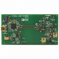
EVAL-ADT7411EBZ Analog Devices Inc, EVAL-ADT7411EBZ Datasheet - Page 29
EVAL-ADT7411EBZ
Manufacturer Part Number
EVAL-ADT7411EBZ
Description
BOARD EVALUATION FOR ADT7411
Manufacturer
Analog Devices Inc
Datasheet
1.ADT7411ARQZ.pdf
(36 pages)
Specifications of EVAL-ADT7411EBZ
Sensor Type
Temperature
Sensing Range
-40°C ~ 120°C
Interface
DSP, I²C, MICROWIRE, QSPI, SMBus, SPI
Sensitivity
±0.5°C
Voltage - Supply
2.7 V ~ 5.5 V
Embedded
No
Utilized Ic / Part
ADT7411
Lead Free Status / RoHS Status
Lead free / RoHS Compliant


SPI Lock Status Register (Read-Only) [Address = 7Fh]
Bit D0 (LSB) of this read-only register indicates whether the SPI
interface is locked or not. Writing to this register causes the
device to malfunction.
Default value is 00h.
0 = I
1 = SPI interface selected and locked.
SERIAL INTERFACE
There are two serial interfaces that can be used on this part: I
and SPI. The device powers up with the serial interface in I
mode, but it is not locked into this mode. To stay in I
is recommended that the user tie the CS line to either V
GND. It is not possible to lock the I
select and lock the SPI mode.
To select and lock the interface into the SPI mode, a number of
pulses must be sent down the CS (Pin 4) line. The following
section describes how this is done.
Once the SPI communication protocol is locked in, it cannot be
unlocked while the device is still powered up. Bit D0 of the SPI
Lock Status register (Address 7Fh) is set to 1 when a successful
SPI interface lock is accomplished. To reset the serial interface,
the user must power down the part and power up again. A
software reset does not reset the serial interface.
Serial Interface Selection
The CS line controls the selection between I
Figure 33 shows the selection process necessary to lock the SPI
interface mode.
To communicate to the ADT7411 using the SPI protocol, send
three pulses down the CS line, as shown in Figure 33. On the
third rising edge (marked as C in Figure 33), the part selects
and locks the SPI interface. Communication to the device is
now limited to the SPI protocol.
As per most SPI standards, the CS line must be low during
every SPI communication to the ADT7411, and high at all other
times. Typical examples of how to connect the dual interface as
I
2
C or SPI are shown in Figure 31 and Figure 32.
2
C interface.
Figure 31. Typical I
ADT7411
SDA
ADD
SCL
CS
I
2
2
V
C ADDRESS = 1001 000
C Interface Connection
DD
10kΩ
2
C mode, but it is possible to
V
DD
10kΩ
2
C and SPI.
2
C mode, it
CC
or
2
C
Rev. B | Page 29 of 36
2
C
The following sections describe in detail how to use the I
SPI protocols associated with the ADT7411.
I
Like all I
address. The four MSBs of this address for the ADT7411 are set
to 1001. The three LSBs are set by Pin 11, ADD. The ADD pin
can be configured three ways to give three different address
options: low, floating, and high. Setting the ADD pin low gives a
serial bus address of 1001 000, leaving it floating gives the
Address 1001 010, and setting it high gives the Address 1001
011. The recommended pull-up resistor value is 10 kΩ.
There is an enable/disable bit for the SMBus timeout. When this
is enabled, the SMBus times out after 25 ms of no activity. To
enable it, set Bit 6 of the Control Configuration 2 register. The
power-up default is with the SMBus timeout disabled.
The ADT7411 supports SMBus packet error checking (PEC)
and its use is optional. It is triggered by supplying the extra
clocks for the PEC byte. The PEC is calculated using CRC-8.
The frame clock sequence (FCS) conforms to CRC-8 by the
polynomial
Consult the SMBus specification for more information.
The serial bus protocol operates as follows:
1.
2
C Serial Interface
ADT7411
C (x) = x
The master initiates a data transfer by establishing a start
condition, defined as a high-to-low transition on the serial
data line SDA while the serial clock line SCL remains high.
This indicates that an address/data stream follows. All slave
peripherals connected to the serial bus respond to the start
condition and shift in the next eight bits, consisting of a
7-bit address (MSB first) plus an R/ W bit, which
determines the direction of the data transfer, that is,
whether data is written to or read from the slave device.
2
C compatible devices, the ADT7411 has a 7-bit serial
DOUT
SCLK
DIN
CS
8
Figure 32. Typical SPI Interface Connection
+ x
2
+ x
820Ω
1
+1
820Ω
V
DD
820Ω
SELECT SPI
LOCK AND
SPI FRAMING
ADT7411
EDGE
2
C and
Related parts for EVAL-ADT7411EBZ
Image
Part Number
Description
Manufacturer
Datasheet
Request
R


Part Number:
Description:
BOARD EVAL FOR SI270X-A
Manufacturer:
Silicon Laboratories Inc
Datasheet:

Part Number:
Description:
BUCK CONV REF DESIGN KIT IP1201
Manufacturer:
International Rectifier
Datasheet:
Part Number:
Description:
BOARD DEMO SYNC DUAL BUCK CNVTER
Manufacturer:
International Rectifier
Datasheet:
Part Number:
Description:
BOARD DEMO SYNC BUCK CONVETER
Manufacturer:
International Rectifier
Datasheet:

Part Number:
Description:
EVALBOARD/EB Omnidirectional microphone - Analog
Manufacturer:
Analog Devices
Datasheet:
Part Number:
Description:
EVALBOARD/EB Omnidirectional microphone - Analog
Manufacturer:
Analog Devices
Datasheet:


Part Number:
Description:
BOARD EVAL LED DRIVER LT3756
Manufacturer:
Linear Technology
Datasheet:

Part Number:
Description:
BOARD EVAL FOR AD7741/7742
Manufacturer:
Analog Devices Inc
Datasheet:

Part Number:
Description:
±1.7g Dual-Axis IMEMS Accelerometer Evaluation Board
Manufacturer:
Analog Devices Inc
Datasheet:

Part Number:
Description:
IC MULTIPLIER ANALOG 8-SOIC T/R
Manufacturer:
Analog Devices Inc
Datasheet:

Part Number:
Description:
IC ANALOG MULTIPLIER 8-DIP
Manufacturer:
Analog Devices Inc
Datasheet:
Part Number:
Description:
IC ANALOG MULTIPLIER 8-SOIC
Manufacturer:
Analog Devices Inc
Datasheet:
Part Number:
Description:
IC ANALOG MULTIPLIER 8-DIP
Manufacturer:
Analog Devices Inc
Datasheet: