EVAL-ADT7411EBZ Analog Devices Inc, EVAL-ADT7411EBZ Datasheet - Page 25
EVAL-ADT7411EBZ
Manufacturer Part Number
EVAL-ADT7411EBZ
Description
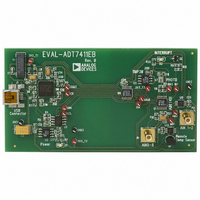
BOARD EVALUATION FOR ADT7411
Manufacturer
Analog Devices Inc
Datasheet
1.ADT7411ARQZ.pdf
(36 pages)
Specifications of EVAL-ADT7411EBZ
Sensor Type
Temperature
Sensing Range
-40°C ~ 120°C
Interface
DSP, I²C, MICROWIRE, QSPI, SMBus, SPI
Sensitivity
±0.5°C
Voltage - Supply
2.7 V ~ 5.5 V
Embedded
No
Utilized Ic / Part
ADT7411
Lead Free Status / RoHS Status
Lead free / RoHS Compliant


Interrupt Mask 2 Register (Read/Write) [Address = 1Eh]
This mask register is an 8-bit read/write register that can be
used to mask out any interrupts that can cause the INT/ INT pin
to go active.
Table 36. Interrupt Mask 2
D7
D7
0
1
Table 37.
Bit
D0
D1
D2
D3
D4
D5:D7
Internal Temperature Offset Register (Read/Write)
[Address = 1Fh]
This register contains the offset value for the internal
temperature channel. A twos complement number can be
written to this register, which is then added to the measured
result before it is stored or compared to limits. In this way, a
sort of one-point calibration can be done whereby the whole
transfer function of the channel can be moved up or down.
From a software point of view, this may be a very simple
method to vary the characteristics of the measurement channel
if the thermal characteristics change. Because it is an 8-bit
register, the temperature resolution is 1°C.
Table 38. Internal Temperature Offset
D7
D7
0
1
External Temperature Offset Register (Read/Write)
[Address = 20h]
This register contains the offset value for the external
temperature channel. A twos complement number can be
written to this register, which is then added to the measured
result before it is stored or compared to limits. In this way, a
sort of one-point calibration can be done whereby the whole
transfer function of the channel can be moved up or down.
From a software point of view, this may be a very simple
method to vary the characteristics of the measurement channel
Default settings at power-up.
Default settings at power-up.
1
1
D6
D6
0
D6
D6
0
1
1
Function
0 = Enable AIN5 interrupt
1 = Disable AIN5 interrupt
0 = Enable AIN6 interrupt
1 = Disable AIN6 interrupt
0 = Enable AIN7 interrupt
1 = Disable AIN7 interrupt
0 = Enable AIN8 interrupt
1 = Disable AIN8 interrupt
0 = Enable V
1 = Disable V
Reserved. Only write 0s
D5
D5
0
D5
D5
0
1
1
D4
D4
0
D4
D4
0
1
1
DD
DD
interrupts
interrupts
D3
D3
0
D3
D3
0
1
1
D2
D2
0
D2
D2
0
1
1
D1
D1
0
D1
D1
0
1
1
D0
D0
0
D0
D0
0
1
1
Rev. B | Page 25 of 36
if the thermal characteristics change. Because it is an 8-bit
register, the temperature resolution is 1°C.
Table 39. External Temperature Offset
D7
D7
0
1
V
This limit register is an 8-bit read/write register that stores the
V
INT/ INT output (if enabled). For this to happen, the measured
V
default value is 5.46 V.
Table 40. V
D7
D7
1
1
V
This limit register is an 8-bit read/write register that stores the
V
INT output (if enabled). For this to happen, the measured V
value has to be less than or equal to the value in this register.
The default value is 2.7 V.
Table 41. V
D7
D7
0
1
Internal T
This limit register is an 8-bit read/write register that stores the
twos complement of the internal temperature upper limit that
causes an interrupt and activates the INT/ INT output (if enabled).
For this to happen, the measured internal temperature value has
to be greater than the value in this register. Because it is an 8-bit
register, the temperature resolution is 1°C. The default value
is 100°C.
Table 42. Internal T
D7
D7
0
1
Default settings at power-up.
Default settings at power-up.
Default settings at power-up.
Default settings at power-up.
1
1
1
1
DD
DD
DD
DD
DD
V
V
upper limit that causes an interrupt and activates the
value has to be greater than the value in this register. The
lower limit that causes an interrupt and activates the INT/
Positive Temperature = Limit Register Code (d)
Negative Temperature = Limit Register Code (d) − 256
HIGH
LOW
D6
D6
0
D6
D6
1
D6
D6
1
D6
D6
1
1
1
Limit Register (Read/Write) [Address = 24h]
1
1
Limit Register (Read/Write) [Address = 23h]
HIGH
DD
DD
V
V
Limit Register (Read/Write) [Address = 25h]
HIGH
LOW
D5
D5
0
D5
D5
0
D5
D5
1
D5
D5
1
1
1
1
1
Limit
Limit
HIGH
D4
D4
0
D4
D4
0
D4
D4
0
D4
D4
0
Limit
1
1
1
1
D3
D3
0
D3
D3
0
D3
D3
0
D3
D3
0
1
1
1
1
D2
D2
0
D2
D2
1
D2
D2
0
D2
D2
1
1
1
1
1
ADT7411
D1
D1
0
D1
D1
1
D1
D1
1
D1
D1
0
1
1
1
1
D0
D0
0
D0
D0
1
D0
D0
0
D0
D0
0
1
1
1
1
DD
Related parts for EVAL-ADT7411EBZ
Image
Part Number
Description
Manufacturer
Datasheet
Request
R


Part Number:
Description:
BOARD EVAL FOR SI270X-A
Manufacturer:
Silicon Laboratories Inc
Datasheet:

Part Number:
Description:
BUCK CONV REF DESIGN KIT IP1201
Manufacturer:
International Rectifier
Datasheet:
Part Number:
Description:
BOARD DEMO SYNC DUAL BUCK CNVTER
Manufacturer:
International Rectifier
Datasheet:
Part Number:
Description:
BOARD DEMO SYNC BUCK CONVETER
Manufacturer:
International Rectifier
Datasheet:

Part Number:
Description:
EVALBOARD/EB Omnidirectional microphone - Analog
Manufacturer:
Analog Devices
Datasheet:
Part Number:
Description:
EVALBOARD/EB Omnidirectional microphone - Analog
Manufacturer:
Analog Devices
Datasheet:


Part Number:
Description:
BOARD EVAL LED DRIVER LT3756
Manufacturer:
Linear Technology
Datasheet:

Part Number:
Description:
BOARD EVAL FOR AD7741/7742
Manufacturer:
Analog Devices Inc
Datasheet:

Part Number:
Description:
±1.7g Dual-Axis IMEMS Accelerometer Evaluation Board
Manufacturer:
Analog Devices Inc
Datasheet:

Part Number:
Description:
IC MULTIPLIER ANALOG 8-SOIC T/R
Manufacturer:
Analog Devices Inc
Datasheet:

Part Number:
Description:
IC ANALOG MULTIPLIER 8-DIP
Manufacturer:
Analog Devices Inc
Datasheet:
Part Number:
Description:
IC ANALOG MULTIPLIER 8-SOIC
Manufacturer:
Analog Devices Inc
Datasheet:
Part Number:
Description:
IC ANALOG MULTIPLIER 8-DIP
Manufacturer:
Analog Devices Inc
Datasheet: