EVAL-ADT7411EBZ Analog Devices Inc, EVAL-ADT7411EBZ Datasheet - Page 5
EVAL-ADT7411EBZ
Manufacturer Part Number
EVAL-ADT7411EBZ
Description
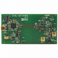
BOARD EVALUATION FOR ADT7411
Manufacturer
Analog Devices Inc
Datasheet
1.ADT7411ARQZ.pdf
(36 pages)
Specifications of EVAL-ADT7411EBZ
Sensor Type
Temperature
Sensing Range
-40°C ~ 120°C
Interface
DSP, I²C, MICROWIRE, QSPI, SMBus, SPI
Sensitivity
±0.5°C
Voltage - Supply
2.7 V ~ 5.5 V
Embedded
No
Utilized Ic / Part
ADT7411
Lead Free Status / RoHS Status
Lead free / RoHS Compliant


Parameter
POWER REQUIREMENTS
1
2
3
4
5
6
7
8
See the Terminology section.
Round robin is the continuous sequential measurement of the following channels: V
AIN6, AIN7, and AIN8.
Guaranteed by design and characterization, not production tested.
The SDA and SCL timing is measured with the input filters turned on so as to meet the fast-mode I
rate but has a negative effect on the EMC behavior of the part.
Guaranteed by design. Not tested in production.
The interface is also capable of handling the I
All input signals are specified with tr = tf = 5 ns (10% to 90% of V
I
DD
V
V
I
I
Power Dissipation
DD
DD
specification is valid for full-scale analog input voltages. Interface inactive. ADC active. Load currents excluded.
DD
DD
(Normal Mode)
(Power-Down Mode)
Settling Time
1
DOUT
SCLK
DIN
CS
8
t
1
D7
X
D6
X
DATA OUT
D5
X
2
DATA IN
C standard mode rise time specification of 1000 ns.
t
2
SDA
SDA
SCL
t
3
D4
Figure 4. Load Circuit for Access Time and Bus Relinquish Time
X
D3
X
Min
2.7
OUTPUT
t
4
t
DD
5
D2
X
Figure 3. SPI Bus Timing Diagram
Figure 2. I
PIN
), and timed from a voltage level of 1.6 V.
TO
50pF
Typ
2.2
D1
X
t
C
1
t
Rev. B | Page 5 of 36
t
6
L
2
2
C Bus Timing Diagram
200µA
200µA
D0
X
Max
5.5
50
3
3
10
10
10
33
DD
D7
X
, internal temperature, external temperature (AIN1, AIN2), AIN3, AIN4, AIN5,
I
I
OL
OH
t
3
D6
t
X
4
Unit
V
ms
mA
mA
μA
μA
mW
μW
2
D5
1.6V
C specification. Switching off the input filters improves the transfer
X
D4
X
Conditions/Comments
V
V
V
V
V
V
V
t
t
DD
DD
DD
DD
DD
DD
DD
6
5
D3
X
settles to within 10% of its final voltage level.
= 3.3 V, V
= 5 V, V
= 3.3 V, V
= 5 V, V
= 3.3 V. Using normal mode.
= 3.3 V. Using shutdown mode.
D2
t
7
X
IH
IH
IH
= V
IH
= V
D1
= V
= V
X
DD
DD
DD
DD
and V
and V
and V
and V
D0
X
t
t
IL
IL
7
8
= GND.
= GND.
IL
IL
= GND.
= GND.
ADT7411
Related parts for EVAL-ADT7411EBZ
Image
Part Number
Description
Manufacturer
Datasheet
Request
R


Part Number:
Description:
BOARD EVAL FOR SI270X-A
Manufacturer:
Silicon Laboratories Inc
Datasheet:

Part Number:
Description:
BUCK CONV REF DESIGN KIT IP1201
Manufacturer:
International Rectifier
Datasheet:
Part Number:
Description:
BOARD DEMO SYNC DUAL BUCK CNVTER
Manufacturer:
International Rectifier
Datasheet:
Part Number:
Description:
BOARD DEMO SYNC BUCK CONVETER
Manufacturer:
International Rectifier
Datasheet:

Part Number:
Description:
EVALBOARD/EB Omnidirectional microphone - Analog
Manufacturer:
Analog Devices
Datasheet:
Part Number:
Description:
EVALBOARD/EB Omnidirectional microphone - Analog
Manufacturer:
Analog Devices
Datasheet:


Part Number:
Description:
BOARD EVAL LED DRIVER LT3756
Manufacturer:
Linear Technology
Datasheet:

Part Number:
Description:
BOARD EVAL FOR AD7741/7742
Manufacturer:
Analog Devices Inc
Datasheet:

Part Number:
Description:
±1.7g Dual-Axis IMEMS Accelerometer Evaluation Board
Manufacturer:
Analog Devices Inc
Datasheet:

Part Number:
Description:
IC MULTIPLIER ANALOG 8-SOIC T/R
Manufacturer:
Analog Devices Inc
Datasheet:

Part Number:
Description:
IC ANALOG MULTIPLIER 8-DIP
Manufacturer:
Analog Devices Inc
Datasheet:
Part Number:
Description:
IC ANALOG MULTIPLIER 8-SOIC
Manufacturer:
Analog Devices Inc
Datasheet:
Part Number:
Description:
IC ANALOG MULTIPLIER 8-DIP
Manufacturer:
Analog Devices Inc
Datasheet: