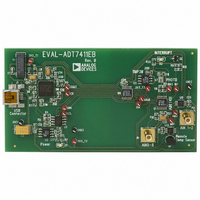
EVAL-ADT7411EBZ Analog Devices Inc, EVAL-ADT7411EBZ Datasheet - Page 32
EVAL-ADT7411EBZ
Manufacturer Part Number
EVAL-ADT7411EBZ
Description
BOARD EVALUATION FOR ADT7411
Manufacturer
Analog Devices Inc
Datasheet
1.ADT7411ARQZ.pdf
(36 pages)
Specifications of EVAL-ADT7411EBZ
Sensor Type
Temperature
Sensing Range
-40°C ~ 120°C
Interface
DSP, I²C, MICROWIRE, QSPI, SMBus, SPI
Sensitivity
±0.5°C
Voltage - Supply
2.7 V ~ 5.5 V
Embedded
No
Utilized Ic / Part
ADT7411
Lead Free Status / RoHS Status
Lead free / RoHS Compliant


ADT7411
The part operates in a slave mode and requires an externally
applied serial clock to the SCLK input. The serial interface is
designed to allow the part to be interfaced to systems that
provide a serial clock that is synchronized to the serial data.
There are two types of serial operation: a read and a write.
Command words are used to distinguish between a read and a
write operation. These command words are given in Table 60.
Address auto-incrementing is possible in SPI mode.
Table 60. SPI Command Words
Write
90h (1001 0000)
Write Operation
Figure 37 shows the timing diagram for a write operation to the
ADT7411. Data is clocked into the registers on the rising edge
of SCLK. When the CS line is high, the DIN and DOUT lines
are in three-state mode. Only when the CS goes from a high to a
low does the part accept any data on the DIN line. In SPI mode,
the address pointer register is capable of auto-incrementing to
the next register in the register map without having to load the
address pointer register each time. In Figure 37, the register
address portion of the diagram gives the first register that is
written to. Subsequent data bytes are written into sequential
writable registers. Therefore, after each data byte is written into
a register, the address pointer register auto-increments its value
to the next available register. The address pointer register auto-
increments from 00h to 3Fh and then loops back to start over
again at 00h.
Read Operation
Figure 38 to Figure 40 show the timing diagrams of correct read
operations. To read back from a register, first write to the
address pointer register with the address to be read from. This
operation is shown in Figure 38. Figure 39 shows the procedure
for reading back a single byte of data. The read command is first
sent to the part during the first eight clock cycles. As the read
command is being sent, irrelevant data is output onto the
DOUT line. During the following eight clock cycles the data
contained in the register selected by the address pointer register
is output onto the DOUT line. Data is output onto the DOUT
line on the falling edge of SCLK. Figure 40 shows the procedure
when reading data from two sequential registers.
Read
91h (1001 0001)
Rev. B | Page 32 of 36
Multiple data reads are possible in SPI interface mode as the
address pointer register is auto-incremental. The address
pointer register auto-increments from 00h to 3Fh and loops
back to start over again at 00h when it reaches 3Fh.
SMBus/SPI INT/ INT
The ADT7411 INT/ INT output is an interrupt line for devices
that want to trade their ability to master for an extra pin. The
ADT7411 is a slave-only device and uses the SMBus/SPI
INT/ INT to signal the host device that it wants to talk. The
SMBus/SPI INT/ INT on the ADT7411 is used as an over/under
limit indicator.
The INT/ INT pin has an open-drain configuration that allows the
outputs of several devices to be wired-AND together when the
INT/ INT pin is active low. Use C6 of the Control Configuration 1
register to set the active polarity of the INT/ INT output. The
power-up default is active low. The INT/ INT output can be
disabled or enabled by setting C5 of the Control Configuration 1
register to 1 or 0, respectively.
The INT/ INT output becomes active when either the internal
temperature value, the external temperature value, V
any of the AIN input values exceed the values in their
corresponding T
INT/ INT output goes inactive again when a conversion result is
the measured value back within the trip limits and when the
status register associated with the out-of-limit event is read. The
two interrupt status registers show which event caused the
INT/ INT pin to go active.
The INT/ INT output requires an external pull-up resistor. This
can be connected to a voltage different from V
maximum voltage rating of the INT/ INT output pin is not
exceeded. The value of the pull-up resistor depends on the
application but should be large enough to avoid excessive sink
currents at the INT/ INT output, which can heat the chip and
affect the temperature reading.
SMBus Alert Response
The INT/ INT pin behaves the same way as an SMBus alert pin
when the SMBus/I
output and requires a pull-up to V
can be wire-AND together so that the common line goes low if
one or more of the INT/ INT outputs goes low. The polarity of
the INT/ INT pin must be set for active low for a number of
outputs to be wire-AND together.
HIGH
2
C interface is selected. It is an open-drain
/V
HIGH
or T
LOW
DD
/V
. Several INT/ INT outputs
LOW
registers. The
DD
, provided the
DD
value, or
Related parts for EVAL-ADT7411EBZ
Image
Part Number
Description
Manufacturer
Datasheet
Request
R


Part Number:
Description:
BOARD EVAL FOR SI270X-A
Manufacturer:
Silicon Laboratories Inc
Datasheet:

Part Number:
Description:
BUCK CONV REF DESIGN KIT IP1201
Manufacturer:
International Rectifier
Datasheet:
Part Number:
Description:
BOARD DEMO SYNC DUAL BUCK CNVTER
Manufacturer:
International Rectifier
Datasheet:
Part Number:
Description:
BOARD DEMO SYNC BUCK CONVETER
Manufacturer:
International Rectifier
Datasheet:

Part Number:
Description:
EVALBOARD/EB Omnidirectional microphone - Analog
Manufacturer:
Analog Devices
Datasheet:
Part Number:
Description:
EVALBOARD/EB Omnidirectional microphone - Analog
Manufacturer:
Analog Devices
Datasheet:


Part Number:
Description:
BOARD EVAL LED DRIVER LT3756
Manufacturer:
Linear Technology
Datasheet:

Part Number:
Description:
BOARD EVAL FOR AD7741/7742
Manufacturer:
Analog Devices Inc
Datasheet:

Part Number:
Description:
±1.7g Dual-Axis IMEMS Accelerometer Evaluation Board
Manufacturer:
Analog Devices Inc
Datasheet:

Part Number:
Description:
IC MULTIPLIER ANALOG 8-SOIC T/R
Manufacturer:
Analog Devices Inc
Datasheet:

Part Number:
Description:
IC ANALOG MULTIPLIER 8-DIP
Manufacturer:
Analog Devices Inc
Datasheet:
Part Number:
Description:
IC ANALOG MULTIPLIER 8-SOIC
Manufacturer:
Analog Devices Inc
Datasheet:
Part Number:
Description:
IC ANALOG MULTIPLIER 8-DIP
Manufacturer:
Analog Devices Inc
Datasheet: