EVAL-ADT7411EBZ Analog Devices Inc, EVAL-ADT7411EBZ Datasheet - Page 19
EVAL-ADT7411EBZ
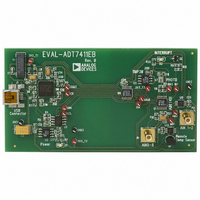
Manufacturer Part Number
EVAL-ADT7411EBZ
Description
BOARD EVALUATION FOR ADT7411
Manufacturer
Analog Devices Inc
Datasheet
1.ADT7411ARQZ.pdf
(36 pages)
Specifications of EVAL-ADT7411EBZ
Sensor Type
Temperature
Sensing Range
-40°C ~ 120°C
Interface
DSP, I²C, MICROWIRE, QSPI, SMBus, SPI
Sensitivity
±0.5°C
Voltage - Supply
2.7 V ~ 5.5 V
Embedded
No
Utilized Ic / Part
ADT7411
Lead Free Status / RoHS Status
Lead free / RoHS Compliant


5.
6.
7.
Because the measurement technique uses switched current
sources, excessive cable and/or filter capacitance can affect the
measurement. When using long cables, the filter capacitor can
be reduced or removed.
Cable resistance can also introduce errors. A series resistance of
1 Ω introduces about 0.5°C error.
Temperature Value Format
One LSB of the ADC corresponds to 0.25°C. The ADC can
theoretically measure a temperature span of 255°C. The internal
temperature sensor is guaranteed to a low value limit of −40°C.
It is possible to measure the full temperature span using the
external temperature sensor. The temperature data format is
shown in Table 6.
The result of the internal or external temperature measurements is
stored as twos complement format in the temperature value
registers and is compared with limits programmed into the
internal or external high and low registers.
Table 6. Temperature Data Format (Internal and External
Temperature)
Temperature (°C)
−40
−25
−10
−0.25
0
+0.25
+10
+25
+50
+75
+100
+105
+125
Temperature Conversion Formula:
1
DB9 is removed from the ADC Code.
Place 0.1 μF bypass and 2200 pF input filter capacitors
close to the ADT7411.
If the distance to the remote sensor is more than 8 inches,
the use of twisted-pair cable is recommended. This works
up to about 6 feet to 12 feet.
For long distances (up to 100 feet) use shielded twisted-
pair cable, such as Belden #8451 microphone cable.
Connect the twisted pair to D+ and D− and the shield to
GND close to the ADT7411. Leave the remote end of the
shield unconnected to avoid ground loops.
Positive Temperature = ADC Code/4
Negative Temperature = (ADC Code
Digital Output
11 0110 0000
11 1001 1100
11 1101 1000
11 1111 1111
00 0000 0000
00 0000 0001
00 0010 1000
00 0110 0100
00 1100 1000
01 0010 1100
01 1001 0000
01 1010 0100
01 1111 0100
1
− 512)/4
Rev. B | Page 19 of 36
Interrupts
The measured results from the internal temperature sensor,
external temperature sensor, V
compared with their T
and T
interrupt occurs if the measurement exceeds or equals the limit
registers. These limits are stored in on-chip registers. Note that
the limit registers are eight bits long while the conversion results
are 10 bits long. If the limits are not masked out, then any out-
of-limit comparisons generate flags that are stored in the
Interrupt Status 1 register (Address 00h) and the Interrupt
Status 2 register (Address 01h). One or more out-of limit results
causes the INT/ INT output to pull either high or low depending
on the output polarity setting. It is good design practice to mask
out interrupts for channels that are of no concern to the
application.
Figure 27 shows the interrupt structure for the ADT7411.
It gives a block diagram representation of how the various
measurement channels affect the INT/ INT pin.
ADT7411 REGISTERS
The ADT7411 contains registers that are used to store the
results of external and internal temperature measurements, V
value measurements, analog input measurements, high and low
temperature limits, supply voltage and analog input limits,
configure multipurpose pins, and generally control the device.
See Table 7 for a detailed description of these registers.
The register map is divided into registers of 8 bits. Each register
has its own individual address but some consist of data that is
linked with other registers. These registers hold the 10-bit
conversion results of measurements taken on the temperature,
V
measurement are stored in Register Address 06h while the two
LSBs are stored in Register Address 03h. The link involved
between these types of registers is that when the LSB register is
read first, the MSB registers associated with that LSB register
are locked out to prevent any updates. To unlock these MSB
registers the user has only to read any one of them, which has
the effect of unlocking all previously locked out MSB registers.
Therefore, for the example given above, if Register 03h is read
first, MSB Register 06h and Register 07h would be locked out to
prevent any updates to them. If Register 06h is read this register,
then Register 07h would be subsequently unlocked.
DD
, and AIN channels. For example, the MSBs of the V
LOW
/V
FIRST READ
COMMAND
LOW
(less than or equal to comparison) limits. An
Figure 29. Phase 1 of 10-Bit Read
HIGH
LOCK ASSOCIATED
MSB REGISTERS
/V
REGISTER
HIGH
LSB
DD
(greater than comparison)
pin, and AIN inputs are
OUTPUT
DATA
ADT7411
DD
DD
Related parts for EVAL-ADT7411EBZ
Image
Part Number
Description
Manufacturer
Datasheet
Request
R


Part Number:
Description:
BOARD EVAL FOR SI270X-A
Manufacturer:
Silicon Laboratories Inc
Datasheet:

Part Number:
Description:
BUCK CONV REF DESIGN KIT IP1201
Manufacturer:
International Rectifier
Datasheet:
Part Number:
Description:
BOARD DEMO SYNC DUAL BUCK CNVTER
Manufacturer:
International Rectifier
Datasheet:
Part Number:
Description:
BOARD DEMO SYNC BUCK CONVETER
Manufacturer:
International Rectifier
Datasheet:

Part Number:
Description:
EVALBOARD/EB Omnidirectional microphone - Analog
Manufacturer:
Analog Devices
Datasheet:
Part Number:
Description:
EVALBOARD/EB Omnidirectional microphone - Analog
Manufacturer:
Analog Devices
Datasheet:


Part Number:
Description:
BOARD EVAL LED DRIVER LT3756
Manufacturer:
Linear Technology
Datasheet:

Part Number:
Description:
BOARD EVAL FOR AD7741/7742
Manufacturer:
Analog Devices Inc
Datasheet:

Part Number:
Description:
±1.7g Dual-Axis IMEMS Accelerometer Evaluation Board
Manufacturer:
Analog Devices Inc
Datasheet:

Part Number:
Description:
IC MULTIPLIER ANALOG 8-SOIC T/R
Manufacturer:
Analog Devices Inc
Datasheet:

Part Number:
Description:
IC ANALOG MULTIPLIER 8-DIP
Manufacturer:
Analog Devices Inc
Datasheet:
Part Number:
Description:
IC ANALOG MULTIPLIER 8-SOIC
Manufacturer:
Analog Devices Inc
Datasheet:
Part Number:
Description:
IC ANALOG MULTIPLIER 8-DIP
Manufacturer:
Analog Devices Inc
Datasheet: