EVAL-ADT7411EBZ Analog Devices Inc, EVAL-ADT7411EBZ Datasheet - Page 23
EVAL-ADT7411EBZ
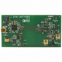
Manufacturer Part Number
EVAL-ADT7411EBZ
Description
BOARD EVALUATION FOR ADT7411
Manufacturer
Analog Devices Inc
Datasheet
1.ADT7411ARQZ.pdf
(36 pages)
Specifications of EVAL-ADT7411EBZ
Sensor Type
Temperature
Sensing Range
-40°C ~ 120°C
Interface
DSP, I²C, MICROWIRE, QSPI, SMBus, SPI
Sensitivity
±0.5°C
Voltage - Supply
2.7 V ~ 5.5 V
Embedded
No
Utilized Ic / Part
ADT7411
Lead Free Status / RoHS Status
Lead free / RoHS Compliant


AIN6 Register MSBs (Read) [Address = 0Dh]
This 8-bit read register contains the eight MSBs of the AIN6
analog input voltage word. The value in this register is combined
with Bit D2 and Bit D3 of the AIN5 to AIN8 register LSBs,
Address 05h, to give the full 10-bit conversion result of the
analog value on the AIN6 pin.
Table 25. AIN6 MSBs
D7
MSB
0
1
AIN7 Register MSBs (Read) [Address = 0Eh]
This 8-bit read register contains the eight MSBs of the AIN7
analog input voltage word. The value in this register is combined
with Bit D4 and Bit D5 of the AIN5 to AIN8 register LSBs,
Address 05h, to give the full 10-bit conversion result of the
analog value on the AIN7 pin.
Table 26. AIN7 MSBs
D7
MSB
0
1
AIN8 Register MSBs (Read) [Address = 0Fh]
This 8-bit read register contains the eight MSBs of the AIN8
analog input voltage word. The value in this register is
combined with Bit D6 and Bit D7 of the AIN5 to AIN8 register
LSBs, Address 05h, to give the full 10-bit conversion result of
the analog value on the AIN8 pin.
Table 27. AIN8 MSBs
D7
MSB
0
1
Control Configuration 1 Register (Read/Write)
[Address = 18h]
This configuration register is an 8-bit read/write register that is
used to set up some of the operating modes of the ADT7411.
Table 28. Control Configuration 1
D7
PD
0
1
Default settings at power-up.
Default settings at power-up.
Default settings at power-up.
Default settings at power-up.
1
1
1
1
D6
C6
0
1
D6
A8
0
D6
A8
0
D6
A8
0
1
1
1
D5
C5
0
1
D5
A7
0
D5
A7
0
D5
A7
0
1
1
1
D4
C4
0
1
D4
A6
0
D4
A6
0
D4
A6
0
1
1
1
D3
C3
1
D3
A5
0
D3
A5
0
D3
A5
0
1
1
1
1
D2
C2
0
D2
A4
0
D2
A4
0
D2
A4
0
1
1
1
1
D1
C1
0
D1
A3
0
D1
A3
0
D1
A3
0
1
1
1
1
D0
C0
0
D0
A2
0
D0
A2
0
D0
A2
0
1
1
1
1
Rev. B | Page 23 of 36
Table 29.
Bit
C0
C2:C1
C3
C4
C5
C6
PD
Control Configuration 2 Register (Read/Write)
[Address = 19h]
This configuration register is an 8-bit read/write register that is
used to set up some of the operating modes of the ADT7411.
Table 30. Control Configuration 2
D7
C7
0
1
Default settings at power-up.
1
D6
C6
0
Function
This bit enables/disables conversions in round robin
and single-channel mode. ADT7411 powers up in round
robin mode, but monitoring is not initiated until this bit
is set. Default = 0.
0 = Stop monitoring.
1 = Start monitoring.
Selects between the two different analog inputs on
Pin 7 and Pin 8. The ADT7411 powers up with AIN1 and
AIN2 selected.
00: AIN1 and AIN2 selected.
01: Undefined.
10: External TDM selected.
11: Undefined.
Reserved. Write 1 only to this bit.
Reserved. Write 0 only.
0: Enable INT/INT output.
1: Disable INT/INT output.
Configures INT/INT output polarity.
0: Active low.
1: Active high.
Power-Down Bit. Setting this bit to 1 puts the ADT7411
into standby mode. In this mode, the analog circuitry
is fully powered down, but the serial interface is still
operational. To power up the part again, write 0 to this bit.
1
D5
C5
0
1
D4
C4
0
1
D3
C3
0
1
D2
C2
0
1
ADT7411
D1
C1
0
1
D0
C0
0
1
Related parts for EVAL-ADT7411EBZ
Image
Part Number
Description
Manufacturer
Datasheet
Request
R


Part Number:
Description:
BOARD EVAL FOR SI270X-A
Manufacturer:
Silicon Laboratories Inc
Datasheet:

Part Number:
Description:
BUCK CONV REF DESIGN KIT IP1201
Manufacturer:
International Rectifier
Datasheet:
Part Number:
Description:
BOARD DEMO SYNC DUAL BUCK CNVTER
Manufacturer:
International Rectifier
Datasheet:
Part Number:
Description:
BOARD DEMO SYNC BUCK CONVETER
Manufacturer:
International Rectifier
Datasheet:

Part Number:
Description:
EVALBOARD/EB Omnidirectional microphone - Analog
Manufacturer:
Analog Devices
Datasheet:
Part Number:
Description:
EVALBOARD/EB Omnidirectional microphone - Analog
Manufacturer:
Analog Devices
Datasheet:


Part Number:
Description:
BOARD EVAL LED DRIVER LT3756
Manufacturer:
Linear Technology
Datasheet:

Part Number:
Description:
BOARD EVAL FOR AD7741/7742
Manufacturer:
Analog Devices Inc
Datasheet:

Part Number:
Description:
±1.7g Dual-Axis IMEMS Accelerometer Evaluation Board
Manufacturer:
Analog Devices Inc
Datasheet:

Part Number:
Description:
IC MULTIPLIER ANALOG 8-SOIC T/R
Manufacturer:
Analog Devices Inc
Datasheet:

Part Number:
Description:
IC ANALOG MULTIPLIER 8-DIP
Manufacturer:
Analog Devices Inc
Datasheet:
Part Number:
Description:
IC ANALOG MULTIPLIER 8-SOIC
Manufacturer:
Analog Devices Inc
Datasheet:
Part Number:
Description:
IC ANALOG MULTIPLIER 8-DIP
Manufacturer:
Analog Devices Inc
Datasheet: