M30260F6AGP#U5A Renesas Electronics America, M30260F6AGP#U5A Datasheet - Page 205
M30260F6AGP#U5A
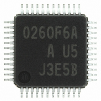
Manufacturer Part Number
M30260F6AGP#U5A
Description
IC M16C MCU FLASH 48K 48LQFP
Manufacturer
Renesas Electronics America
Series
M16C™ M16C/Tiny/26r
Datasheet
1.M30260F3AGPU5A.pdf
(354 pages)
Specifications of M30260F6AGP#U5A
Core Processor
M16C/60
Core Size
16-Bit
Speed
20MHz
Connectivity
I²C, IEBus, SIO, UART/USART
Peripherals
DMA, PWM, Voltage Detect, WDT
Number Of I /o
39
Program Memory Size
48KB (48K x 8)
Program Memory Type
FLASH
Ram Size
2K x 8
Voltage - Supply (vcc/vdd)
2.7 V ~ 5.5 V
Data Converters
A/D 12x10b
Oscillator Type
Internal
Operating Temperature
-20°C ~ 85°C
Package / Case
48-LQFP
Cpu Family
R8C
Device Core Size
16b
Frequency (max)
20MHz
Interface Type
UART
Total Internal Ram Size
2KB
# I/os (max)
39
Number Of Timers - General Purpose
8
Operating Supply Voltage (typ)
3.3/5V
Operating Supply Voltage (max)
5.5V
Operating Supply Voltage (min)
3V
On-chip Adc
12-chx10-bit
Instruction Set Architecture
CISC
Operating Temp Range
-20C to 85C
Operating Temperature Classification
Commercial
Mounting
Surface Mount
Pin Count
48
Package Type
LQFP
Package
48LQFP
Family Name
R8C
Maximum Speed
20 MHz
Operating Supply Voltage
3.3|5 V
Data Bus Width
16 Bit
Number Of Programmable I/os
39
Number Of Timers
8
For Use With
R0K33026AS000BE - KIT DEV EVALUATION M16C/26A
Lead Free Status / RoHS Status
Lead free / RoHS Compliant
Eeprom Size
-
Lead Free Status / Rohs Status
Compliant
Available stocks
Company
Part Number
Manufacturer
Quantity
Price

Part Number:
M30260F6AGP#U5AM30260F6AGP#D3
Manufacturer:
Renesas Electronics America
Quantity:
10 000
Part Number:
M30260F6AGP#U5AM30260F6AGP#U3
Manufacturer:
Renesas Electronics America
Quantity:
10 000
Part Number:
M30260F6AGP#U5AM30260F6AGP#U3A
Manufacturer:
Renesas Electronics America
Quantity:
10 000


M
R
R
14.1 Operation Modes
e
E
1
. v
J
6
Table 14.1.1.1 One-shot Mode Specifications
Figure 14.1.1.1 Operation Example in One-Shot Mode
0
C
14.1.1 One-Shot Mode
A/D Conversion Start
Condition
A/D Conversion Stop
Condition
Interrupt Request Generation Timing A/D conversion completed
2
Function
Analog Input Pin
Readout of A/D Conversion Result
9
2 /
0 .
B
In one-shot mode, analog voltage applied to a selected pin is once converted to a digital code. Table
14.1.1.1 shows the one-shot mode specifications. Figure 14.1.1.1 shows the operation example in one-
shot mode. Figure 14.1.1.2 shows the ADCON0 to ADCON2 registers in one-shot mode.
0
0
6
2
A
0
F
AN
AN
AN
AN
AN
AN
AN
AN
2
G
e
•Example when selecting AN
0 -
b
o r
0
1
2
3
4
5
6
7
1 .
2
Item
u
0
, 5
A/D conversion started
0
p
2
(
0
M
0
1
7
6
C
page 186
2 /
6
, A
A/D interrupt request generated
M
The CH2 to CH0 bits in the ADCON0 register and the ADGSEL1 to
ADGSEL0 bits in the ADCON2 register select pins. Analog voltage applied to
a selected pin is once converted to a digital code
• When the TRG bit in the ADCON0 register is “0” (software trigger)
• When the TRG bit in the ADCON0 register is “1” (hardware trigger)
• A/D conversion completed (If a software trigger is selected, the ADST bit is
• Set the ADST bit to “0”
Select one pin from AN
Readout one of the AD0 to AD7 registers that corresponds to the selected pin
1
The AD
ADST bit to “1” (A/D conversion started)
Set the ADST bit in the ADCON0 register to “1” (A/D conversion started)
set to “0” (A/D conversion halted)).
f o
6
C
3
2 /
2
___________
9
6
, B
TRG
2
M
to an analog input pin (Ch2 to CH0=010
1
pin input changes state from “H” to “L” after setting the
6
C
2 /
6
) T
0
to AN
Specification
7
, AN
30
to AN
32
, AN
24
2
A/D pin input voltage
sampling
)
A/D pin conversion
14. A/D Converter
Related parts for M30260F6AGP#U5A
Image
Part Number
Description
Manufacturer
Datasheet
Request
R

Part Number:
Description:
KIT STARTER FOR M16C/29
Manufacturer:
Renesas Electronics America
Datasheet:

Part Number:
Description:
KIT STARTER FOR R8C/2D
Manufacturer:
Renesas Electronics America
Datasheet:

Part Number:
Description:
R0K33062P STARTER KIT
Manufacturer:
Renesas Electronics America
Datasheet:

Part Number:
Description:
KIT STARTER FOR R8C/23 E8A
Manufacturer:
Renesas Electronics America
Datasheet:

Part Number:
Description:
KIT STARTER FOR R8C/25
Manufacturer:
Renesas Electronics America
Datasheet:

Part Number:
Description:
KIT STARTER H8S2456 SHARPE DSPLY
Manufacturer:
Renesas Electronics America
Datasheet:

Part Number:
Description:
KIT STARTER FOR R8C38C
Manufacturer:
Renesas Electronics America
Datasheet:

Part Number:
Description:
KIT STARTER FOR R8C35C
Manufacturer:
Renesas Electronics America
Datasheet:

Part Number:
Description:
KIT STARTER FOR R8CL3AC+LCD APPS
Manufacturer:
Renesas Electronics America
Datasheet:
Part Number:
Description:
KIT STARTER FOR RX610
Manufacturer:
Renesas Electronics America
Datasheet:

Part Number:
Description:
KIT STARTER FOR R32C/118
Manufacturer:
Renesas Electronics America
Datasheet:

Part Number:
Description:
KIT DEV RSK-R8C/26-29
Manufacturer:
Renesas Electronics America
Datasheet:

Part Number:
Description:
KIT STARTER FOR SH7124
Manufacturer:
Renesas Electronics America
Datasheet:

Part Number:
Description:
KIT STARTER FOR H8SX/1622
Manufacturer:
Renesas Electronics America
Datasheet:

Part Number:
Description:
KIT DEV FOR SH7203
Manufacturer:
Renesas Electronics America
Datasheet: