DF2166VT33V Renesas Electronics America, DF2166VT33V Datasheet
DF2166VT33V
Specifications of DF2166VT33V
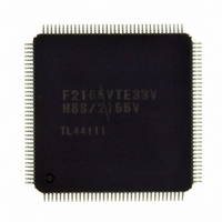
DF2166VTE33V
HD64F2166VTE33V
HD64F2166VTE33V
Available stocks


Related parts for DF2166VT33V


DF2166VT33V Summary of contents
Page 1
To our customers, Old Company Name in Catalogs and Other Documents st On April 1 , 2010, NEC Electronics Corporation merged with Renesas Technology Corporation, and Renesas Electronics Corporation took over all the business of both companies. Therefore, although the ...
Page 2
All information included in this document is current as of the date this document is issued. Such information, however, is subject to change without any prior notice. Before purchasing or using any Renesas Electronics products listed herein, please confirm ...
Page 3
H8S/2168Group 16 Hardware Manual Renesas 16-Bit Single-Chip Microcomputer H8S Family / H8S/2100 Series The revision list can be viewed directly by clicking the title page. The revision list summarizes the locations of revisions and additions. Details should always be checked ...
Page 4
Rev. 3.00, 03/04, page ...
Page 5
Keep safety first in your circuit designs! 1. Renesas Technology Corp. puts the maximum effort into making semiconductor products better and more reliable, but there is always the possibility that trouble may occur with them. Trouble with semiconductors may lead ...
Page 6
General Precautions on Handling of Product 1. Treatment of NC Pins Note: Do not connect anything to the NC pins. The NC (not connected) pins are either not connected to any of the internal circuitry or are used as test ...
Page 7
Configuration of This Manual This manual comprises the following items: 1. General Precautions on Handling of Product 2. Configuration of This Manual 3. Preface 4. Contents 5. Overview 6. Description of Functional Modules • CPU and System-Control Modules • On-Chip ...
Page 8
This LSI is a microcomputer (MCU) made up of the H8S/2000 CPU with Renesas Technology's original architecture as its core, and the peripheral functions required to configure a system server. The H8S/2000 CPU has an internal 32-bit configuration, ...
Page 9
In order to understand the details of the CPU's functions Read the H8S/2600 Series, H8S/2000 Series Programming Manual. • In order to understand the detailed function of a register whose name is known Read the index that is the ...
Page 10
Rev. 3.00, 03/04, page viii of xl ...
Page 11
Section 1 Overview............................................................................................1 1.1 Overview........................................................................................................................... 1 1.2 Internal Block Diagram..................................................................................................... 2 1.3 Pin Description.................................................................................................................. 3 1.3.1 Pin Arrangement .................................................................................................. 3 1.3.2 Pin Arrangement in Each Operating Mode.......................................................... 4 1.3.3 Pin Functions ....................................................................................................... 9 Section 2 CPU....................................................................................................15 2.1 Features............................................................................................................................. 15 2.1.1 ...
Page 12
Effective Address Calculation ............................................................................. 47 2.8 Processing States............................................................................................................... 49 2.9 Usage Notes ...................................................................................................................... 51 2.9.1 Note on TAS Instruction Usage........................................................................... 51 2.9.2 Note on Bit Manipulation Instructions ................................................................ 51 2.9.3 EEPMOV Instruction........................................................................................... 52 Section 3 MCU Operating Modes ..................................................................... ...
Page 13
External Interrupts ............................................................................................... 82 5.4.2 Internal Interrupts ................................................................................................ 84 5.5 Interrupt Exception Handling Vector Table...................................................................... 85 5.6 Interrupt Control Modes and Interrupt Operation ............................................................. 88 5.6.1 Interrupt Control Mode 0 ..................................................................................... 90 5.6.2 Interrupt Control Mode 1 ..................................................................................... 92 ...
Page 14
Section 7 Data Transfer Controller (DTC)........................................................ 149 7.1 Features............................................................................................................................. 149 7.2 Register Descriptions........................................................................................................ 151 7.2.1 DTC Mode Register A (MRA) ............................................................................ 152 7.2.2 DTC Mode Register B (MRB)............................................................................. 153 7.2.3 DTC Source Address Register (SAR).................................................................. 153 7.2.4 DTC Destination Address ...
Page 15
Section 8 I/O Ports .............................................................................................177 8.1 Port 1................................................................................................................................. 183 8.1.1 Port 1 Data Direction Register (P1DDR)............................................................. 183 8.1.2 Port 1 Data Register (P1DR)................................................................................ 184 8.1.3 Port 1 Pull-Up MOS Control Register (P1PCR).................................................. 184 8.1.4 Pin Functions ....................................................................................................... 185 8.1.5 Port ...
Page 16
Port 8 Data Register (P8DR) ............................................................................... 217 8.8.3 Pin Functions ....................................................................................................... 218 8.9 Port 9................................................................................................................................. 222 8.9.1 Port 9 Data Direction Register (P9DDR)............................................................. 222 8.9.2 Port 9 Data Register (P9DR) ............................................................................... 223 8.9.3 Pin Functions ....................................................................................................... 223 8.10 Port ...
Page 17
Section 9 8-Bit PWM Timer (PWM).................................................................251 9.1 Features............................................................................................................................. 251 9.2 Input/Output Pins .............................................................................................................. 252 9.3 Register Descriptions ........................................................................................................ 252 9.3.1 PWM Register Select (PWSL)............................................................................. 253 9.3.2 PWM Data Registers (PWDR15 to PWDR0).......................................... 255 9.3.3 PWM Data Polarity ...
Page 18
Input Capture Input Timing ................................................................................. 292 11.5.5 Buffered Input Capture Input Timing .................................................................. 293 11.5.6 Timing of Input Capture Flag (ICF) Setting ........................................................ 294 11.5.7 Timing of Output Compare Flag (OCF) setting................................................... 295 11.5.8 Timing of FRC Overflow Flag ...
Page 19
Usage Notes ...................................................................................................................... 330 12.9.1 Conflict between TCNT Write and Counter Clear............................................... 330 12.9.2 Conflict between TCNT Write and Increment..................................................... 331 12.9.3 Conflict between TCOR Write and Compare-Match........................................... 332 12.9.4 Conflict between Compare-Matches A and B ..................................................... 333 12.9.5 ...
Page 20
Data Transfer Format........................................................................................... 381 14.4.2 Receive Data Sampling Timing and Reception Margin in Asynchronous Mode ................................................................................................................... 382 14.4.3 Clock.................................................................................................................... 383 14.4.4 Serial Enhanced Mode Clock .............................................................................. 383 14.4.5 SCI Initialization (Asynchronous Mode)............................................................. 386 14.4.6 Serial Data Transmission (Asynchronous Mode) ...
Page 21
Features................................................................................................................ 428 14.11.2 Register Descriptions........................................................................................... 428 14.11.3 CRC Operation Circuit Operation........................................................................ 430 14.11.4 Note on CRC Operation Circuit........................................................................... 433 2 Section Bus Interface (IIC) .....................................................................435 15.1 Features............................................................................................................................. 435 15.2 Input/Output Pins .............................................................................................................. 438 15.3 Register Descriptions ...
Page 22
Bidirectional Data Registers (TWR0 to TWR15).................................... 528 16.3.9 Status Registers (STR1 to STR3) .............................................................. 529 16.3.10 SERIRQ Control Register 0 (SIRQCR0)............................................................. 536 16.3.11 SERIRQ Control Register 1 (SIRQCR1)............................................................. 539 16.3.12 SERIRQ Control Register ...
Page 23
Usage Note........................................................................................................................ 594 Section 18 A/D Converter..................................................................................595 18.1 Features............................................................................................................................. 595 18.1.1 Block Diagram..................................................................................................... 596 18.2 Input/Output Pins .............................................................................................................. 597 18.3 Register Descriptions ........................................................................................................ 598 18.3.1 A/D Data Registers (ADDRA to ADDRD) ............................................. 598 18.3.2 A/D Control/Status ...
Page 24
Hardware Protection ............................................................................................ 665 20.5.2 Software Protection ............................................................................................. 666 20.5.3 Error Protection ................................................................................................... 666 20.6 Switching between User MAT and User Boot MAT........................................................ 668 20.7 Programmer Mode ............................................................................................................ 669 20.8 Serial Communication Interface Specification for Boot Mode......................................... 670 20.9 ...
Page 25
Module Stop Control Registers H, L, and A (MSTPCRH, MSTPCRL, MSTPCRA) ............................................................... 732 23.1.4 Sub-Chip Module Stop Control Registers BH, BL (SUBMSTPBH, SUBMSTPBL) ......................................................................... 734 23.1.5 Sub-Chip Module Stop Control Registers AH, AL (SUBMSTPAH, SUBMSTPAL) ......................................................................... 734 23.2 Mode ...
Page 26
Appendix ......................................................................................................... 817 A. I/O Port States in Each Pin State....................................................................................... 817 B. Product Lineup.................................................................................................................. 819 C. Package Dimensions ......................................................................................................... 820 Main Revisions and Additions in this Edition..................................................... 821 Index ......................................................................................................... 825 Rev. 3.00, 03/04, page xxiv of xl ...
Page 27
Section 1 Overview Figure 1.1 Internal Block Diagram ................................................................................................. 2 Figure 1.2 Pin Arrangement (TFP-144).......................................................................................... 3 Section 2 CPU Figure 2.1 Exception Vector Table (Normal Mode)..................................................................... 19 Figure 2.2 Stack Structure in Normal Mode ................................................................................. 19 Figure 2.3 Exception Vector ...
Page 28
Section 6 Bus Controller (BSC) Figure 6.1 Block Diagram of Bus Controller.............................................................................. 103 Figure 6.2 IOS Signal Output Timing ........................................................................................ 123 Figure 6.3 Access Sizes and Data Alignment Control (8-bit Access Space).............................. 124 Figure 6.4 Access Sizes and Data Alignment ...
Page 29
Figure 7.11 DTC Operation Timing (Example of Chain Transfer) ............................................ 171 Section 8 I/O Ports Figure 8.1 Noise Canceler Circuit .............................................................................................. 208 Figure 8.2 Noise Canceler Operation.......................................................................................... 208 Section 9 8-Bit PWM Timer (PWM) Figure 9.1 Block Diagram of PWM ...
Page 30
Section 12 8-Bit Timer (TMR) Figure 12.1 Block Diagram of 8-Bit Timer (TMR_0 and TMR_1)............................................ 306 Figure 12.2 Block Diagram of 8-Bit Timer (TMR_Y and TMR_X).......................................... 307 Figure 12.3 Pulse Output Example ............................................................................................. 322 Figure 12.4 Count Timing for Internal ...
Page 31
Figure 14.11 Example of SCI Operation in Reception (Example with 8-Bit Data, Parity, One Stop Bit)................................................... 389 Figure 14.12 Sample Serial Reception Flowchart (1)................................................................. 391 Figure 14.12 Sample Serial Reception Flowchart (2)................................................................. 392 Figure 14.13 Example of Communication Using Multiprocessor ...
Page 32
Figure 14.47 MSB-First Data Transmission............................................................................... 430 Figure 14.48 LSB-First Data Reception ..................................................................................... 431 Figure 14.49 MSB-First Data Reception .................................................................................... 432 Figure 14.50 LSB-First and MSB-First Transmit Data .............................................................. 433 2 Section Bus Interface (IIC) Figure 15.1 Block ...
Page 33
Figure 15.29 Notes on Reading Master Receive Data ................................................................ 500 Figure 15.30 Flowchart for Start Condition Issuance Instruction for Retransmission and Timing............................................................................................................. 501 Figure 15.31 Stop Condition Issuance Timing ........................................................................... 502 Figure 15.32 IRIC Flag Clearing Timing When WAIT = ...
Page 34
Figure 20.7 Automatic-Bit-Rate Adjustment Operation of SCI ................................................. 639 Figure 20.8 Overview of Boot Mode State Transition Diagram................................................. 641 Figure 20.9 Programming/Erasing Overview Flow.................................................................... 642 Figure 20.10 RAM Map When Programming/Erasing is Executed ........................................... 643 Figure 20.11 Programming Procedure........................................................................................ 644 ...
Page 35
Figure 25.6 Oscillation Stabilization Timing (Exiting Software Standby Mode)....................... 790 Figure 25.7 External Clock Input Timing................................................................................... 790 Figure 25.8 Timing of External Clock Output Stabilization Delay Time ................................... 791 Figure 25.9 Subclock Input Timing ............................................................................................ 791 Figure 25.10 Reset Input ...
Page 36
Rev. 3.00, 03/04, page xxxiv of xl ...
Page 37
Section 1 Overview Table 1.1 Pin Arrangement in Each Operating Mode............................................................... 4 Table 1.2 Pin Functions ............................................................................................................ 9 Section 2 CPU Table 2.1 Instruction Classification ........................................................................................ 31 Table 2.2 Operation Notation ................................................................................................. 32 Table 2.3 Data Transfer Instructions....................................................................................... 33 Table ...
Page 38
Table 5.8 Number of States in Interrupt Handling Routine Execution Status ........................ 96 Table 5.9 Interrupt Source Selection and Clearing Control .................................................... 98 Section 6 Bus Controller (BSC) Table 6.1 Pin Configuration.................................................................................................. 104 Table 6.2 Address Ranges and External Address ...
Page 39
Table 8.1 Port Functions (cont) ............................................................................................ 180 Table 8.1 Port Functions (cont) ............................................................................................ 181 Table 8.1 Port Functions (cont) ............................................................................................ 182 Table 8.2 Port 1 Input Pull-Up MOS States.......................................................................... 186 Table 8.3 Port 2 Input Pull-Up MOS States.......................................................................... 190 Table ...
Page 40
Section 14 Serial Communication Interface (SCI, IrDA, and CRC) Table 14.1 Pin Configuration.................................................................................................. 355 Table 14.2 Relationships between N Setting in BRR and Bit Rate B..................................... 369 Table 14.3 Examples of BRR Settings for Various Bit Rates (Asynchronous Mode) (1) ...
Page 41
Table 16.7 Fast A20 Gate Output Signals............................................................................... 576 Table 16.8 Scope of LPC Interface Pin Shutdown ................................................................. 578 Table 16.9 Scope of Initialization in Each LPC Interface Mode ............................................ 579 Table 16.10 Serial Interrupt Transfer Cycle Frame Configuration ....................................... 582 ...
Page 42
Section 23 Power-Down Modes Table 23.1 Operating Frequency and Wait Time.................................................................... 730 Table 23.2 LSI Internal States in Each Mode ......................................................................... 737 Section 25 Electrical Characteristics Table 25.1 Absolute Maximum Ratings ................................................................................. 783 Table 25.2 DC Characteristics (1) .......................................................................................... 784 ...
Page 43
Overview • High-speed H8S/2000 central processing unit with an internal 16-bit architecture Upward-compatible with H8/300 and H8/300H CPUs on an object level Sixteen 16-bit general registers 65 basic instructions • Various peripheral functions Data transfer controller (DTC) 8-bit PWM ...
Page 44
Package Code TQFP-144 TFP-144 1.2 Internal Block Diagram XTAL EXTAL PFSEL MD2 MD1 MD0 RES RESO STBY FWE NMI ETRST ETMS ETDO ETDI ETCK LWR/P90 AH/P91 CPCS1/P92 RD/P93 HWR/P94 IOS/AS/P95 EXCL/φ/P96 CS256/WAIT/P97 D0/KIN0/FTCI/P60 D1/KIN1/FTOA/P61 D2/KIN2/FTIA/P62 D3/KIN3/FTIB/P63 D4/KIN4/FTIC/P64 D5/KIN5/FTID/P65 D6/KIN6/FTOB/P66 D7/KIN7/P67 ...
Page 45
Pin Description 1.3.1 Pin Arrangement 108 107106 105 104 103102 101 100 ...
Page 46
Pin Arrangement in Each Operating Mode Table 1.1 Pin Arrangement in Each Operating Mode Pin No. Pin Name Extended Mode TFP- 144 (EXPE = 1) 1 VCC 2 P45/IRQ5/TMIY 3 P46/IRQ6/TMOX 4 P47/IRQ7/TMOY 5 P56/IRQ14/PWX0 6 P57/IRQ15/PWX1 7 VSS ...
Page 47
Pin No. Pin Name Extended Mode TFP- 144 (EXPE = 1) 28 PC4/SCL4 29 PC3/SDA3 30 PC2/SCL3 31 PC1/SDA2 32 PC0/SCL2 33 PA7/A23/KIN15/EVENT7 34 PA6/A22/KIN14/EVENT6 35 PA5/A21/KIN13/EVENT5 36 VCC 37 PA4/A20/KIN12/EVENT4 38 PA3/A19/KIN11/EVENT3 39 PA2/A18/KIN10/EVENT2 40 PA1/A17/KIN9/EVENT1/SSE2I 41 PA0/A16/KIN8/EVENT0/SSE0I 42 ...
Page 48
Pin No. Pin Name Extended Mode TFP- 144 (EXPE = 1) 59 PD7/SDA5 60 PD6/SCL5 61 PD5/LPCPD 62 PD4/CLKRUN 63 PD3/GA20 64 PD2/PME 65 PD1/LSMI 66 PD0/LSCI 67 AVSS 68 P70/AN0 69 P71/AN1 70 P72/ExIRQ2/AN2 71 P73/ExIRQ3/AN3 72 P74/ExIRQ4/AN4 73 ...
Page 49
Pin No. Pin Name Extended Mode TFP- 144 (EXPE = 1) 90 ETCK ETRST 91 92 PF2/ExPW2 93 PF1/ExPW1 94 PF0/ExPW0 95 VSS 96 P27/A15/AD15 97 P26/A14/AD14 98 P25/A13/AD13 99 P24/A12/AD12 100 P23/A11/AD11 101 P22/A10/AD10 102 P21/A9/AD9 103 P20/A8/AD8 104 ...
Page 50
Pin No. Pin Name TFP- 144 Extended Mode 121 P30/D8/WUE8 122 P31/D9/WUE9 123 P32/D10/WUE10 124 P33/D11/WUE11 125 P34/D12/WUE12 126 P35/D13/WUE13 127 P36/D14/WUE14 128 P37/D15/WUE15 129 P40/IRQ0/TMI0 130 P41/IRQ1/TMI1 131 P42/IRQ2/TMO0 132 P43/IRQ3/TMO1 133 P52/IRQ10/TxD1/IrTxD 134 P53/IRQ11/RxD1/IrRxD 135 FWE 136 P54/IRQ12/TxD2 ...
Page 51
Pin Functions Table 1.2 Pin Functions Type Symbol Pin No. Power VCC 1, 36 supply 86 VCL 13 VSS 7, 42, 95, 111 139 Clock XTAL 143 EXTAL 144 φ 18 EXCL 18 PFSEL 141 MD2 Operating 14 mode ...
Page 52
Type Symbol Pin No. Address/ AD15 103 data AD8 multiplex AD7 to 104 to 110, bus AD0 112 WAIT Bus control HWR 20 LWR 24 AS/IOS 19 CS256 17 CPCS1 Interrupts ...
Page 53
Type Symbol Pin No. PWM timer PW15 110 (PWM) PW0 112 ExPW2 ExPW0 14-bit PWM PWX0 5 timer PWX1 6 (PWMX) PWX2 26 PWX3 25 16-bit free FTCI 78 running FTOA 79 timer ...
Page 54
Type Symbol Pin No. KIN15 to Keyboard KIN13 control KIN12 KIN8 KIN7 KIN0 WUE15 to 128 to 121 Input WUE8 A/D AN7 converter AN0 (ADC) ...
Page 55
Type Symbol Pin No. LPC LAD3 Interface LAD0 (LPC) LFRAME 54 LRESET 53 LCLK 52 SERIRQ 51 LSCI, 66 LSMI, 65 PME 64 GA20 63 CLKRUN 62 LPCPD 61 Event EVENT15 113 to 120, Counter to ...
Page 56
Type Symbol I/O ports P17 to P10 P27 to P20 P37 to P30 P47 to P40 P57 to P50 P67 to P60 P77 to P70 P87 to P80 P97 to P90 PA7 to PA0 PB7 to PB0 PC7 to PC0 ...
Page 57
The H8S/2000 CPU is a high-speed central processing unit with an internal 32-bit architecture that is upward-compatible with the H8/300 and H8/300H CPUs. The H8S/2000 CPU has sixteen 16-bit general registers, can address a 16 Mbytes linear address space, and ...
Page 58
Two CPU operating modes Normal mode* Advanced mode Note: * Not available in this LSI. • Power-down state Transition to power-down state by SLEEP instruction Selectable CPU clock speed 2.1.1 Differences between H8S/2600 CPU and ...
Page 59
Differences from H8/300 CPU In comparison to the H8/300 CPU, the H8S/2000 CPU has the following enhancements. • More general registers and control registers Eight 16-bit extended registers and one 8-bit control register have been added. • Extended ...
Page 60
CPU Operating Modes The H8S/2000 CPU has two operating modes: normal* and advanced. Normal mode* supports a maximum 64 kbytes address space. Advanced mode supports a maximum 16 Mbytes address space. The mode is selected by the LSI's mode ...
Page 61
H'0000 Reset exception vector H'0001 H'0002 (Reserved for system use) H'0003 H'0004 H'0005 (Reserved for system use) H'0006 H'0007 H'0008 Exception vector 1 H'0009 H'000A Exception vector 2 H'000B Figure 2.1 Exception Vector Table (Normal Mode (16 bits) ...
Page 62
Advanced Mode • Address space Linear access to a maximum address space of 16 Mbytes is possible. • Extended registers (En) The extended registers (E0 to E7) can be used as 16-bit registers. They can also be used as ...
Page 63
The memory indirect addressing mode (@@aa:8) employed in the JMP and JSR instructions uses an 8-bit absolute address included in the instruction code to specify a memory operand that contains a branch address. In advanced mode, the operand is a ...
Page 64
Address Space Figure 2.5 shows a memory map of the H8S/2000 CPU. The H8S/2000 CPU provides linear access to a maximum 64 kbytes address space in normal mode, and a maximum 16 Mbytes (architecturally 4 Gbytes) address space in ...
Page 65
Register Configuration The H8S/2000 CPU has the internal registers shown in figure 2.6. There are two types of registers: general registers and control registers. Control registers are a 24-bit program counter (PC), an 8-bit extended control register (EXR), and ...
Page 66
General Registers The H8S/2000 CPU has eight 32-bit general registers. These general registers are all functionally alike and can be used as both address registers and data registers. When a general register is used as a data register, it ...
Page 67
SP (ER7) 2.4.2 Program Counter (PC) This 24-bit counter indicates the address of the next instruction the CPU will execute. The length of all CPU instructions is 2 bytes (one word), so the least significant PC bit is ignored. (When ...
Page 68
Condition-Code Register (CCR) This 8-bit register contains internal CPU status information, including an interrupt mask bit (I) and half-carry (H), negative (N), zero (Z), overflow (V), and carry (C) flags. Operations can be performed on the CCR bits by ...
Page 69
Bit Bit Name Initial Value 0 C Undefined 2.4.5 Initial Register Values Reset exception handling loads the CPU's program counter (PC) from the vector table, clears the trace (T) bit in EXR to 0, and sets the interrupt mask (I) ...
Page 70
Data Formats The H8S/2000 CPU can process 1-bit, 4-bit BCD, 8-bit (byte), 16-bit (word), and 32-bit (longword) data. Bit-manipulation instructions operate on 1-bit data by accessing bit … byte operand data. ...
Page 71
Data Type Register Number Word data Rn Word data En 15 MSB Longword data ERn 31 MSB En [Legend] ERn: General register ER En: General register E Rn: General register R RnH: General register RH RnL: General register RL MSB: ...
Page 72
Memory Data Formats Figure 2.10 shows the data formats in memory. The H8S/2000 CPU can access word data and longword data in memory, but word or longword data must begin at an even address attempt is made ...
Page 73
Instruction Set The H8S/2000 CPU has 65 types of instructions. The instructions are classified by function as shown in table 2.1. Table 2.1 Instruction Classification Function Instructions Data transfer MOV 1 POP* , PUSH* LDM, STM* MOVFPE* Arithmetic ADD, ...
Page 74
Table of Instructions Classified by Function Tables 2.3 to 2.10 summarize the instructions in each functional category. The notation used in tables 2.3 to 2.10 is defined below. Table 2.2 Operation Notation Symbol Description Rd General register (destination)* Rs ...
Page 75
Table 2.3 Data Transfer Instructions 1 Instruction Size* Function (EAs) → Rd, Rs → (EAd) MOV B/W/L Moves data between two general registers or between a general register and memory, or moves immediate data to a general register. MOVFPE B ...
Page 76
Table 2.4 Arithmetic Operations Instructions (1) Instruction Size* Function Rd ± Rs → Rd, Rd ± #IMM → Rd ADD B/W/L SUB Performs addition or subtraction on data in two general registers immediate data and data in a ...
Page 77
Table 2.4 Arithmetic Operations Instructions (2) Instruction Size* Function Rd ÷ Rs → Rd DIVXS B/W Performs signed division on data in two general registers: either 16 bits ÷ 8 bits → 8-bit quotient and 8-bit remainder or 32 bits ...
Page 78
Table 2.5 Logic Operations Instructions Instruction Size* Function Rd ∧ Rs → Rd, Rd ∧ #IMM → Rd AND B/W/L Performs a logical AND operation on a general register and another general register or immediate data. Rd ∨ Rs → ...
Page 79
Table 2.7 Bit Manipulation Instructions (1) Instruction Size* Function 1 → (<bit-No.> of <EAd>) BSET B Sets a specified bit in a general register or memory operand to 1. The bit number is specified by 3-bit immediate data or the ...
Page 80
Table 2.7 Bit Manipulation Instructions (2) Instruction Size* Function C ⊕ (<bit-No.> of <EAd>) → C BXOR B Logically exclusive-ORs the carry flag with a specified bit in a general register or memory operand and stores the result in the ...
Page 81
Table 2.8 Branch Instructions Instruction Size Function Bcc – Branches to a specified address if a specified condition is true. The branching conditions are listed below. Mnemonic BRA (BT) BRN (BF) BHI BLS BCC (BHS) BCS (BLO) BNE BEQ BVC ...
Page 82
Table 2.9 System Control Instructions Instruction Size* Function TRAPA – Starts trap-instruction exception handling. RTE – Returns from an exception-handling routine. SLEEP – Causes a transition to a power-down state. (EAs) → CCR, (EAs) → EXR LDC B/W Moves the ...
Page 83
Table 2.10 Block Data Transfer Instructions Instruction Size Function if R4L ≠ 0 then EEPMOV.B – else next ≠ 0 then EEPMOV.W – else next: Transfers a data block. Starting from the address set in ER5, transfers data ...
Page 84
Operation field only (2) Operation field and register fields op (3) Operation field, register fields, and effective address extension (4) Operation field, effective address extension, and condition field op Figure 2.11 Instruction Formats (Examples) Rev. 3.00, 03/04, page 42 ...
Page 85
Addressing Modes and Effective Address Calculation The H8S/2000 CPU supports the eight addressing modes listed in table 2.11. Each instruction uses a subset of these addressing modes. Arithmetic and logic operations instructions can use the register direct and immediate ...
Page 86
Register Indirect—@ERn The register field of the instruction code specifies an address register (ERn) which contains the address of a memory operand. If the address is a program instruction address, the lower 24 bits are valid and the upper ...
Page 87
Table 2.12 Absolute Address Access Ranges Absolute Address Data address 8 bits (@aa:8) 16 bits (@aa:16) 32 bits (@aa:32) Program instruction 24 bits (@aa:24) address Note: Not available in this LSI. * 2.7.6 Immediate—#xx:8, #xx:16, or #xx:32 The 8-bit (#xx:8), ...
Page 88
Memory Indirect—@@aa:8 This mode can be used by the JMP and JSR instructions. The instruction code contains an 8-bit absolute address specifying a memory operand which contains a branch address. The upper bits of the 8-bit absolute address are ...
Page 89
Effective Address Calculation Table 2.13 indicates how effective addresses are calculated in each addressing mode. In normal mode*, the upper eight bits of the effective address are ignored in order to generate a 16-bit address. Note * Not available ...
Page 90
Table 2.13 Effective Address Calculation (2) Addressing Mode and Instruction Format Absolute address Immediate Note: Not available in this LSI. * Rev. 3.00, 03/04, page 48 of 830 Effective Address Calculation PC contents Sign extension Memory contents Memory contents Effective ...
Page 91
Processing States The H8S/2000 CPU has five main processing states: the reset state, exception handling state, program execution state, bus-released state, and program stop state. Figure 2.13 indicates the state transitions. • Reset state In this state the CPU ...
Page 92
End of bus request Bus-released state End of exception handling Exception-handling state RES = high *1 Reset state From any state except hardware standby mode, a transition to the reset state occurs whenever RES Notes: 1. goes low. A transition ...
Page 93
Usage Notes 2.9.1 Note on TAS Instruction Usage The TAS instruction is not generated by the Renesas H8S and H8/300 series C/C++ compilers. The TAS instruction can be used as a user-defined intrinsic function. 2.9.2 Note on Bit Manipulation ...
Page 94
EEPMOV Instruction 1. EEPMOV is a block-transfer instruction and transfers the byte size of data indicated by R4*, which starts from the address indicated by ER5, to the address indicated by ER6. ER5 ER5 + R4* 2. Set R4* ...
Page 95
Section 3 MCU Operating Modes 3.1 Operating Mode Selection This LSI supports one operating mode (mode 2). The operating mode is determined by the setting of the mode pins (MD2, MD1, and MD0). Table 3.1 shows the MCU operating mode ...
Page 96
Register Descriptions The following registers are related to the operating mode. For details on the bus control register (BCR), see section 6.3.1, Bus Control Register (BCR), and for details on bus control register 2 (BCR2), see section 6.3.2, Bus ...
Page 97
System Control Register (SYSCR) SYSCR selects a system pin function, monitors a reset source, selects the interrupt control mode and the detection edge for NMI, enables or disables register access to the on-chip peripheral modules, and enables or disables ...
Page 98
Bit Bit Name Initial Value 1 KINWUE 0 0 RAME 1 3.2.3 Serial Timer Control Register (STCR) STCR enables or disables register access, IIC operating mode, and on-chip flash memory, and selects the input clock of the timer counter. Bit ...
Page 99
Bit Bit Name Initial Value 4 IICE 0 3 FLSHE 0 2 — ICKS1 0 0 ICKS0 0 R/W Description R/W IIC Master Enable Enables or disables CPU access for IIC registers (ICCR, ICSR, ICDR/SARX, ICMR/SAR), PWMX registers ...
Page 100
Operating Mode Descriptions 3.3.1 Mode 2 The CPU can access a 16 Mbytes address space in advanced mode. The on-chip ROM is enabled. After a reset, the LSI is set to single-chip mode. To access an external address space, ...
Page 101
Table 3.2 Pin Functions in Each Mode Port Normal extension Port 1 I/O port* or Address bus output Port 2 I/O port* or Address bus output Port 3 I/O port* or Data bus I/O Port 6 I/O port* or Data ...
Page 102
Address Map Figures 3.1 to 3.3 show memory maps in operating mode. ROM: 256 kbytes, RAM: 40 kbytes Mode 2 (EXPE = 1) Advanced mode Extended mode with on-chip ROM H'000000 H'03FFFF H'07FFFF H'080000 H'F7FFFF H'F80000 H'FBFFFF H'FC0000 H'FEFFFF ...
Page 103
ROM: 384 kbytes, RAM: 40 kbytes Mode 2 (EXPE = 1) Advanced mode Extended mode with on-chip ROM H'000000 On-chip ROM H'05FFFF Reserved area H'07FFFF H'080000 External address H'F7FFFF H'F80000 256 kbytes H'FBFFFF extended area H'FC0000 External address H'FEFFFF H'FF0000 ...
Page 104
ROM: 512 kbytes, RAM: 40 kbytes Mode 2 (EXPE = 1) Advanced mode Extended mode with on-chip ROM H'000000 H'07FFFF H'080000 H'F7FFFF H'F80000 H'FBFFFF H'FC0000 H'FEFFFF H'FF0000 H'FF07FF H'FF0800 H'FF97FF H'FF9800 H'FFBFFF H'FFC000 H'FFDFFF H'FFE000 H'FFE07F H'FFE080 H'FFEFFF H'FFF000 H'FFF7FF ...
Page 105
Section 4 Exception Handling 4.1 Exception Handling Types and Priority As table 4.1 indicates, exception handling may be caused by a reset, interrupt, direct transition, or trap instruction. Exception handling is prioritized as shown in table 4.1. If two or ...
Page 106
Exception Sources and Exception Vector Table Different vector addresses are assigned to different exception sources. Table 4.2 lists the exception sources and their vector addresses. Table 4.2 Exception Handling Vector Table Exception Source Reset Reserved for system use Direct ...
Page 107
Table 4.2 Exception Handling Vector Table (cont) Exception Source Internal interrupt* External interrupt IRQ8 IRQ9 IRQ10 IRQ11 IRQ12 IRQ13 IRQ14 IRQ15 Internal interrupt* Note: For details on the internal interrupt vector table, see section 5.5, Interrupt Exception * Handling Vector ...
Page 108
Reset A reset has the highest exception priority. When the RES pin goes low, all processing halts and this LSI enters the reset. To ensure that this LSI is reset, hold the RES pin low for at least 20 ...
Page 109
RES Internal address bus Internal read signal Internal write signal Internal data bus (1) Reset exception handling vector address ( H'000000 ( H'000002 (2) Start address (contents of reset exception handling vector address) (3) Start ...
Page 110
Interrupt Exception Handling Interrupts are controlled by the interrupt controller. The sources to start interrupt exception handling are external interrupt sources (NMI, IRQ15 to IRQ0, KIN15 to KIN0, and WUE15 to WUE8) and internal interrupt sources from the on-chip ...
Page 111
Stack Status after Exception Handling Figure 4.2 shows the stack after completion of trap instruction exception handling and interrupt exception handling. Figure 4.2 Stack Status after Exception Handling Advanced mode SP CCR PC (24 bits) Rev. 3.00, 03/04, page ...
Page 112
Usage Note When accessing word data or longword data, this LSI assumes that the lowest address bit is 0. The stack should always be accessed in words or longwords, and the value of the stack pointer (SP: ER7) should ...
Page 113
Section 5 Interrupt Controller 5.1 Features • Two interrupt control modes Any of two interrupt control modes can be set by means of the INTM1 and INTM0 bits in the system control register (SYSCR). • Priorities settable with ICR An ...
Page 114
SYSCR NMI input IRQ input KIN input WUE input Internal interrupt sources SWDTEND to IBFI3 Interrupt controller [Legend] ICR: Interrupt control register ISCR: IRQ sense control register IER: IRQ enable register ISR: IRQ status register KMIMR: Keyboard matrix interrupt mask ...
Page 115
Input/Output Pins Table 5.1 summarizes the pins of the interrupt controller. Table 5.1 Pin Configuration Symbol I/O NMI Input IRQ15 to IRQ0 Input ExIRQ15 to ExIRQ2 KIN15 to KIN0 Input WUE15 to WUE8 Input Function Nonmaskable external interrupt Rising ...
Page 116
Register Descriptions The interrupt controller has the following registers. For details on the system control register (SYSCR), see section 3.2.2, System Control Register (SYSCR), and for details on the IRQ sense port select registers (ISSR16, ISSR), see section 8.16.1, ...
Page 117
Table 5.2 Correspondence between Interrupt Source and ICR Bit Bit Name ICRA 7 ICRn7 IRQ0 6 ICRn6 IRQ1 5 ICRn5 IRQ2, IRQ3 4 ICRn4 IRQ4, IRQ5 3 ICRn3 IRQ6, IRQ7 2 ICRn2 DTC 1 ICRn1 WDT_0 0 ICRn0 WDT_1 [Legend]] ...
Page 118
Break Address Registers (BARA to BARC) The BAR registers specify an address that break address. An address in which the first byte of an instruction exists should be set as a break ...
Page 119
IRQ Sense Control Registers (ISCR16H, ISCR16L, ISCRH, ISCRL) The ISCR registers select the source that generates an interrupt request at pins IRQ15 to IRQ0 or pins ExIRQ15 to ExIRQ2. • ISCR16H Bit Bit Name Initial Value 7 IRQ15SCB 0 ...
Page 120
ISCRH Bit Bit Name Initial Value 7 IRQ7SCB 0 6 IRQ7SCA 0 5 IRQ6SCB 0 4 IRQ6SCA 0 3 IRQ5SCB 0 2 IRQ5SCA 0 1 IRQ4SCB 0 0 IRQ4SCA 0 • ISCRL Bit Bit Name Initial Value 7 IRQ3SCB ...
Page 121
IRQ Enable Registers (IER16, IER) The IER registers control the enabling and disabling of interrupt requests IRQ15 to IRQ0. • IER16 Bit Bit Name Initial Value IRQ15E to All 0 IRQ8E • IER Bit Bit Name ...
Page 122
IRQ Status Registers (ISR16, ISR) The ISR registers are flag registers that indicate the status of IRQ15 to IRQ0 interrupt requests. • ISR16 Bit Bit Name Initial Value IRQ15F to All 0 IRQ8F • ISR Bit ...
Page 123
Keyboard Matrix Interrupt Mask Registers (KMIMRA, KMIMR6) Wake-Up Event Interrupt Mask Register (WUEMR3) The KMIMR and WUEMR registers enable or disable key-sensing interrupt inputs (KIN15 to KIN0), and wake-up event interrupt inputs (WUE15 to WUE8). The KMIMRA, KMIMR6, and ...
Page 124
Interrupt Sources 5.4.1 External Interrupts There are four external interrupts: NMI, IRQ15 to IRQ0, KIN15 to KIN0 and WUE15 to WUE8. These interrupts can be used to restore this LSI from software standby mode. NMI Interrupt: NMI is the ...
Page 125
KIN15 to KIN0 Interrupts, WUE15 to WUE8 Interrupts: Interrupts KIN15 to KIN0 and WUE15 to WUE8 are requested by an input signal at pins KIN15 to KIN0 and WUE15 to WUE8. Interrupts KIN15 to KIN0 and WUE15 to WUE8 have ...
Page 126
Internal Interrupts Internal interrupts issued from the on-chip peripheral modules have the following features: • For each on-chip peripheral module there are flags that indicate the interrupt request status, and enable bits that individually select enabling or disabling of ...
Page 127
Interrupt Exception Handling Vector Table Table 5.3 lists interrupt exception handling sources, vector addresses, and interrupt priorities. For default priorities, the lower the vector number, the higher the priority. Modules set at the same priority will conform to their ...
Page 128
Table 5.3 Interrupt Sources, Vector Addresses, and Interrupt Priorities (cont) Origin of Interrupt Source Name FRT ICIA (Input capture A) ICIB (Input capture B) ICIC (Input capture C) ICID (Input capture D) OCIA (Output compare A) OCIB (Output compare B) ...
Page 129
Table 5.3 Interrupt Sources, Vector Addresses, and Interrupt Priorities (cont) Origin of Interrupt Source Name IIC_0 IICI0 IIC_1 IICI1 IIC_4 IICI4 IIC_5 IICI5 LPC ERR1(transfer error, etc.) IBFI1 (IDR1 reception completion) IBFI2 (IDR2 reception completion) IBFI3 (IDR3 reception completion) Vector ...
Page 130
Interrupt Control Modes and Interrupt Operation The interrupt controller has two modes: Interrupt control mode 0 and interrupt control mode 1. Interrupt operations differ depending on the interrupt control mode. NMI interrupts and address break interrupts are always accepted ...
Page 131
Interrupt Acceptance Control and 3-Level Control: In interrupt control modes 0 and 1, interrupt acceptance control and 3-level mask control is performed by means of the I and UI bits in CCR and ICR (control level). Table 5.5 shows the ...
Page 132
Table 5.6 Operations and Control Signal Functions in Each Interrupt Control Mode Setting Interrupt Control Mode INTM1 INTM0 [Legend] O: Interrupt operation control performed IM: Used as an interrupt mask bit PR: Sets priority —: ...
Page 133
An interrupt with interrupt control level 1? IRQ0 Yes Figure 5.5 Flowchart of Procedure up to Interrupt Acceptance in Interrupt Control Mode 0 Program execution state Interrupt generated? Yes Yes NMI No No Yes No IRQ0 No Yes IRQ1 Yes ...
Page 134
Interrupt Control Mode 1 In interrupt control mode 1, mask control is applied to three levels for IRQ and on-chip peripheral module interrupt requests by comparing the I and UI bits in CCR in the CPU, and the ICR ...
Page 135
If an interrupt source occurs when the corresponding interrupt enable bit is set interrupt request is sent to the interrupt controller. 2. According to the interrupt control level specified in ICR, the interrupt controller only accepts ...
Page 136
An interrupt with interrupt control level 1? IRQ0 Yes Figure 5.7 Flowchart of Procedure Up to Interrupt Acceptance in Interrupt 5.6.3 Interrupt Exception Handling Sequence Figure 5.8 shows the interrupt exception handling sequence. The example shown is for the case ...
Page 137
Figure 5.8 Interrupt Exception Handling Rev. 3.00, 03/04, page 95 of 830 ...
Page 138
Interrupt Response Times Table 5.7 shows interrupt response times − the intervals between generation of an interrupt request and execution of the first instruction in the interrupt handling routine. The execution status symbols used in table 5.7 are explained ...
Page 139
DTC Activation by Interrupt The DTC can be activated by an interrupt. In this case, the following options are available: • Interrupt request to CPU • Activation request to DTC • Both of the above For details of interrupt ...
Page 140
Operation Order: If the same interrupt is selected as a DTC activation source and a CPU interrupt source, the DTC data transfer is performed first, followed by CPU interrupt exception handling. Table 5.9 summarizes interrupt source selection and interrupt source ...
Page 141
Usage Notes 5.7.1 Conflict between Interrupt Generation and Disabling When an interrupt enable bit is cleared disable interrupt requests, the disabling becomes effective after execution of the instruction. When an interrupt enable bit is cleared to ...
Page 142
Instructions that Disable Interrupts The instructions that disable interrupts are LDC, ANDC, ORC, and XORC. After any of these instructions are executed, all interrupts including NMI are disabled and the next instruction is always executed. When the I bit ...
Page 143
Section 6 Bus Controller (BSC) This LSI has an on-chip bus controller (BSC) that manages the bus width and the number of access states of the external address space. The BSC also has a bus arbitration function, and controls the ...
Page 144
Multiplex bus interface Address 256-kbyte 2 states * extended area CP extended area 2 states * IOS extended area 2 states * Note wait cycle is inserted by the setting of the WC22 bit. • Basic bus ...
Page 145
External bus control signals WAIT [Legend] BCR: Bus control register BCR2: Bus control register 2 WSCR: Wait state control register WSCR2: Wait state control register 2 Figure 6.1 Block Diagram of Bus Controller Bus controller BCR BCR2 WSCR WSCR2 Wait ...
Page 146
Input/Output Pins Table 6.1 summarizes the pin configuration of the bus controller. Table 6.1 Pin Configuration Symbol I/O AS Output IOS Output CPCS1 Output CS256 Output RD Output HWR Output LWR Output WAIT Input AH Output AD15 to AD0 ...
Page 147
Register Descriptions The following registers are provided for the bus controller. For the system control register (SYSCR), see section 3.2.2, System Control Register (SYSCR). For system control register 2 (SYSCR2), see section 8.6.4, System Control Register 2 (SYSCR2). • ...
Page 148
Initial Bit Bit Name Value R/W 3 BRSTS0 0 R/W R/W 1 IOS1 1 R/W 0 IOS0 1 R/W 6.3.2 Bus Control Register 2 (BCR2) BCR2 is used to specify the access mode for the CP extended ...
Page 149
Initial Bit Bit Name Value R/W 3 ADFULLE 0 R/W 2 EXCKS 0 R/W R/W 0 CPCSE 0 R/W Description Address Output Full Enable Controls the address output in access to the IOS extended area, 256-kbyte extended ...
Page 150
Wait State Control Register (WSCR) WSCR is used to specify the data bus width, the number of access states, the wait mode, and the number of wait states for access to external address spaces (basic extended area and 256-kbyte ...
Page 151
Initial Bit Bit Name Value R/W 4 AST 1 R/W 3 WMS1 0 R/W 2 WMS0 0 R/W 1 WC1 1 R/W 0 WC0 1 R/W Description Basic Extended Area Access State Control Selects the number of states for access ...
Page 152
Wait State Control Register 2 (WSCR2) WSCR2 is used to specify the wait mode and number of wait states in access to the 256-kbyte extended area and CP extended area. Initial Bit Bit Name Value R/W 7 WMS10 0 ...
Page 153
When ADMXE = 0 Initial Bit Bit Name Value R/W 2 WC22 1 R/W 1 WC21 1 R/W 0 WC20 1 R/W • When ADMXE = 1 Initial Bit Bit Name Value R/W 2 WC22 1 R/W 1 WC21 ...
Page 154
Bus Control 6.4.1 Bus Specifications The external address space bus specifications consist of three elements: bus width, the number of access states, and the wait mode and the number of program wait states. The bus width and the number ...
Page 155
Table 6.2 Address Ranges and External Address Spaces Address Range H'080000 to H'F7FFFF (15 Mbytes) H'F80000 to H'FBFFFF (256 kbytes) 256-kbyte extended area H'FC0000 to H'FEFFFF (192 kbytes) H'FF0800 to H'FFBFFF (46 kbytes) H'FFC000 to H'FFDFFF (8 kbytes) CP extended ...
Page 156
Table 6.3 Bit Settings and Bus Specifications of Basic Bus Interface BRSTRM CS256E CPCSE Note the burst ROM interface, the bus width is specified ...
Page 157
Table 6.4 Bus Specifications for Basic Extended Area/Basic Bus Interface ABW AST WMS1 WMS0 Other than WMS1 = 0 and WMS0 = Other than WMS1 ...
Page 158
Table 6.5 Bus Specifications for 256-kbyte Extended Area/Basic Bus Interface ABW256 AST256 WMS10 [Legend] Don’t care *: Rev. 3.00, 03/04, page 116 of 830 WC11 WC10 Bus Width ...
Page 159
Table 6.6 Bus Specifications for CP Extended Area (Basic Mode)/Basic Bus Interface ABWCP ASTCP WMS21 Other than WMS21 = 0 and WMS20 = Other than WMS21 = 0 and ...
Page 160
In Address-Data Multiplex Extended Mode (a) Bus Width: A bus width bits can be selected via the ABW and ABW256 bits in WSCR, and the ABWCP bit in BCR2. (b) Number of Access States: Two ...
Page 161
Table 6.7 Address-Data Multiplex Address Spaces Address Range H'080000 to H'F7FFFF (15 Mbytes) 256-kbyte extended area H'F80000 to H'F8FFFF (64 kbytes) 256-kbyte extended area H'F90000 to H'F9FFFF (64 kbytes) 256-kbyte extended area H'FA0000 to H'FAFFFF (64 kbytes) 256-kbyte extended area ...
Page 162
Table 6.8 Bit Settings and Bus Specifications of Basic Bus Interface IOSE CS256E CPCSE Table 6.9 Bus Specifications for IOS Extended Area/Multiplex Bus Interface (Address Cycle) ...
Page 163
Table 6.11 Bus Specifications for 256-kbyte Extended Area/Multiplex Bus Interface (Address Cycle) AST256 WMS10 WC22 Table 6.12 Bus Specifications for 256-kbyte Extended Area/Multiplex Bus Interface (Data Cycle) AST256 WMS1 0 — Table 6.13 ...
Page 164
Table 6.14 Bus Specifications for CP Extended Area/Multiplex Bus Interface (Data Cycle) ASTCP WMS21 WMS20 0 — — Other than WMS21 = 0 and WMS20 = 1 6.4.2 Advanced Mode The external address space (H'FFF000 to H'FFF7FF) ...
Page 165
I/O Select Signals The LSI can output I/O select signals (IOS); the signal is driven low when the corresponding external address space is accessed. Figure 6.2 shows an example of IOS signal output timing. φ Address bus IOS Enabling ...
Page 166
Bus Interface The normal extended bus interface enables direct connection to ROM and SRAM. For details on selection of the bus specifications for the basic extended area, 256-kbyte extended area, and CP extended area, see tables 6.4 to 6.6. ...
Page 167
Access Space: Figure 6.4 illustrates data alignment control for the 16-bit access space. With the 16-bit access space, the upper data bus (D15 to D8/AD15 to AD8) and lower data bus (D7 to D0/AD7 to AD0) are used ...
Page 168
Valid Strobes Table 6.16 shows the data buses used and valid strobes for each access space read, the RD signal is valid for both the upper and lower halves of the data bus write, the ...
Page 169
Basic Operation Timing in Normal Extended Mode (1) 8-Bit, 2-State Access Space: Figure 6.5 shows the bus timing for an 8-bit, 2-state access space. When an 8-bit access space is accessed, the upper half (D15 to D8) of the ...
Page 170
Access Space: Figure 6.6 shows the bus timing for an 8-bit, 3-state access space. When an 8-bit access space is accessed, the upper half (D15 to D8) of the data bus is used. Wait states can be ...
Page 171
Access Space: Figures 6.7 to 6.9 show bus timings for a 16-bit, 2-state access space. When a 16-bit access space is accessed, the upper half (D15 to D8) of the data bus is used for even addresses, ...
Page 172
Address bus IOS (IOSE = 1) CS256 (CS256E = 1) CPCS1 (CPCSE = 1) AS (IOSE = D15 to D8 Read HWR LWR Write D15 Note: * For ...
Page 173
Address bus IOS (IOSE = 1) CS256 (CS256E = 1) CPCS1 (CPCSE = 1) AS (IOSE = D15 to D8 Read HWR LWR Write D15 Note: * For ...
Page 174
Access Space: Figures 6.10 to 6.12 show bus timings for a 16-bit, 3-state access space. When a 16-bit access space is accessed, the upper half (D15 to D8) of the data bus is used for even addresses, ...
Page 175
Address bus IOS (IOSE = 1) CS256 (CS256E = 1) CPCS1 (CPCSE = 1) AS (IOSE = D15 to D8 Read HWR LWR Write D15 Note: * For ...
Page 176
Address bus IOS (IOSE = 1) CS256 (CS256E = 1) CPCS1 (CPCSE = 1) AS (IOSE = D15 to D8 Read HWR LWR Write D15 Note: * For ...
Page 177
Basic Operation Timing in Address-Data Multiplex Extended Mode (1) 8-Bit, 2-State Data Access Space: Figures 6.13 and 6.14 show the bus timing for an 8-bit, 2- state access space. When an 8-bit access space is accessed, the upper half ...
Page 178
Data Access Space: Figure 6.15 shows the bus timing for an 8-bit, 3-state access space. When an 8-bit access space is accessed, the upper half (AD15 to AD8) of the data bus is used. Wait states can ...
Page 179
Address φ CPCS1 CS256 IOS AH RD HWR LWR AD15 to AD8 AD7 to AD0 Figure 6.16 Bus Timing for 16-Bit, 2-State Access Space (1) (Even Byte Access) Address T 1 φ CPCS1 CS256 IOS AH RD ...
Page 180
CPCS1 CS256 IOS AH RD HWR LWR AD15 to AD8 AD7 to AD0 Figure 6.18 Bus Timing for 16-Bit, 2-State Access Space (3) (Odd Byte Access) φ CK2S CPCS1 CS256 IOS AH RD HWR LWR AD15 to AD8 AD7 ...
Page 181
Address φ CPCS2 CS256 IOS AH RD HWR LWR AD15 to AD8 Address AD7 to AD0 Address Figure 6.20 Bus Timing for 16-Bit, 2-State Access Space (5) (Word Access) Address T 1 φ CPCS1 CP256 IOS ...
Page 182
Data Access Space: Figures 6.22 to 6.24 show bus timings for a 16-bit, 3-state access space. When a 16-bit access space is accessed, the upper half (AD15 to AD8) of the data bus is used for even ...
Page 183
Address φ CPCS1 CS256 IOS AH RD HWR LWR AD15 to AD8 Address AD7 to AD0 Address Figure 6.24 Bus Timing for 16-Bit, 3-State Access Space (3) (Word Access) 6.5.5 Wait Control When accessing the external ...
Page 184
Pin Auto-Wait Mode: A specified number of wait states T state when accessing the external address space if the WAIT pin is low at the falling edge and φ in the last T state. The number ...
Page 185
In Address-Data Multiplex Extended Mode (a) Program Wait Mode: Program wait mode includes address wait and data wait. 256-kbyte extended area and IOS extended area: Zero or one state of address wait T data wait T is inserted between ...
Page 186
T 3 φ CPCS1 CS256 IOS WAIT AH RD HWR LWR AD15 to AD8 AD7 to AD0 Figure 6.26 Example of Wait State Insertion Timing Rev. 3.00, 03/04, page 144 of 830 Read Cycle Data ...
Page 187
Burst ROM Interface In this LSI, the external address space can be designated as the burst ROM space by the BRSTRM bit in BCR, and the burst ROM interface enabled. Consecutive burst accesses of a maximum four or eight ...
Page 188
Address bus AS/IOS (IOSE = 0) RD Data bus Figure 6.28 Access Timing Example in Burst ROM Space (AST = BRSTS1 = 0) 6.6.2 Wait Control As with the basic bus interface, program wait insertion or pin wait insertion using ...
Page 189
Idle Cycle When this LSI accesses the external address space, it can insert a 1-state idle cycle (T bus cycles when a write cycle occurs immediately after a read cycle. By inserting an idle cycle it is possible, for ...
Page 190
Bus Arbitration 6.8.1 Overview The BSC has a bus arbiter that arbitrates bus master operations. There are two bus masters – the CPU and DTC – that perform read/write operations while they have bus mastership. 6.8.2 Operation Each bus ...
Page 191
Section 7 Data Transfer Controller (DTC) This LSI includes a data transfer controller (DTC). The DTC can be activated by an interrupt or software, to transfer data. Figure 7.1 shows a block diagram of the DTC. The DTC's register information ...
Page 192
Interrupt controller Interrupt request CPU interrupt request [Legend] MRA, MRB: CRA, CRB: SAR: DAR: DTCERA to DTCERE: DTVECR: Rev. 3.00, 03/04, page 150 of 830 Internal address bus DTC Internal data bus DTC mode register A, B DTC transfer count ...
Page 193
Register Descriptions The DTC has the following registers. • DTC mode register A (MRA) • DTC mode register B (MRB) • DTC source address register (SAR) • DTC destination address register (DAR) • DTC transfer count register A (CRA) ...
Page 194
DTC Mode Register A (MRA) MRA selects the DTC operating mode. Initial Bit Bit Name Value 7 SM1 Undefined 6 SM0 5 DM1 Undefined 4 DM0 3 MD1 Undefined 2 MD0 1 DTS Undefined 0 Sz Undefined [Legend] *: ...
Page 195
DTC Mode Register B (MRB) MRB selects the DTC operating mode. Initial Bit Bit Name Value 7 CHNE Undefined 6 DISEL Undefined — Undefined 7.2.3 DTC Source Address Register (SAR) SAR is a 24-bit register that ...
Page 196
DTC Transfer Count Register A (CRA) CRA is a 16-bit register that designates the number of times data transferred by the DTC. In normal mode, the entire CRA functions as a 16-bit transfer counter (1 to ...
Page 197
Table 7.1 Correspondence between Interrupt Sources and DTCER Bit Bit Name DTCERA 7 DTCEn7 (16)IRQ0 6 DTCEn6 (17)IRQ1 5 DTCEn5 (18)IRQ2 4 DTCEn4 (19)IRQ3 3 DTCEn3 (28)ADI 2 DTCEn2 (48)ICIA 1 DTCEn1 (49)ICIB 0 DTCEn0 (52)OCIA [Legend ...
Page 198
Initial Bit Bit Name Value DTVEC6 to All 0 DTVEC0 7.2.9 Keyboard Comparator Control Register (KBCOMP) KBCOMP enables or disables the comparator scan function of event counter. Initial Bit Bit Name Value 7 EVENTE 0 6, ...
Page 199
Event Counter Control Register (ECCR) ECCR selects the event counter channels for use and the detection edge. Initial Bit Bit Name Value 7 EDSB — All ECSB3 to All 0 ECSB0 ...
Page 200
Event Counter Status Register (ECS) ECS is a 16-bit register that holds events temporarily. The DTC decides the counter to be incremented according to the state of this register. Reading this register allows the monitoring of events that are ...