DF2166VT33V Renesas Electronics America, DF2166VT33V Datasheet - Page 511
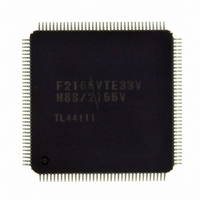
DF2166VT33V
Manufacturer Part Number
DF2166VT33V
Description
IC H8S MCU FLASH 512K 144TQFP
Manufacturer
Renesas Electronics America
Series
H8® H8S/2100r
Specifications of DF2166VT33V
Core Processor
H8S/2000
Core Size
16-Bit
Speed
33MHz
Connectivity
I²C, IrDA, LPC, SCI, SmartCard
Peripherals
POR, PWM, WDT
Number Of I /o
106
Program Memory Size
512KB (512K x 8)
Program Memory Type
FLASH
Ram Size
40K x 8
Voltage - Supply (vcc/vdd)
3 V ~ 3.6 V
Data Converters
A/D 8x10b; D/A 2x8b
Oscillator Type
External
Operating Temperature
-20°C ~ 75°C
Package / Case
144-TQFP, 144-VQFP
Cpu Family
H8S
Device Core Size
16/32Bit
Frequency (max)
33MHz
Interface Type
I2C/IrDA/SCI
Total Internal Ram Size
40KB
# I/os (max)
106
Number Of Timers - General Purpose
5
Operating Supply Voltage (typ)
3.3V
Operating Supply Voltage (max)
3.6V
Operating Supply Voltage (min)
3V
On-chip Adc
8-chx10-bit
On-chip Dac
2-chx8-bit
Instruction Set Architecture
CISC
Operating Temp Range
-20C to 75C
Operating Temperature Classification
Commercial
Mounting
Surface Mount
Pin Count
144
Package Type
TQFP
Package
144TQFP
Family Name
H8S
Maximum Speed
33 MHz
Operating Supply Voltage
3.3 V
Data Bus Width
16|32 Bit
Number Of Programmable I/os
106
Number Of Timers
5
For Use With
HS0005KCU11H - EMULATOR E10A-USB H8S(X),SH2(A)3DK2166 - DEV EVAL KIT H8S/2166
Lead Free Status / RoHS Status
Lead free / RoHS Compliant
Eeprom Size
-
Lead Free Status / Rohs Status
Compliant
Other names
DF2166VTE33V
DF2166VTE33V
HD64F2166VTE33V
HD64F2166VTE33V
DF2166VTE33V
HD64F2166VTE33V
HD64F2166VTE33V
Available stocks
Company
Part Number
Manufacturer
Quantity
Price
Company:

Part Number:
DF2166VT33V
Manufacturer:
Exar
Quantity:
60
Company:
Part Number:
DF2166VT33V
Manufacturer:
Renesas Electronics America
Quantity:
10 000


[1] Initialize the IIC as described in section 15.4.2, Initialization.
[2] Read the BBSY flag in ICCR to confirm that the bus is free.
[3] Set bits MST and TRS to 1 in ICCR to select master transmit mode.
[4] Write 1 to BBSY and 0 to SCP in ICCR. This changes SDA from high to low when SCL is
[5] Then the IRIC and IRTR flags are set to 1. If the IEIC bit in ICCR has been set to 1, an
[6] Write the data (slave address + R/W) to ICDR.
[7] When one frame of data has been transmitted, the IRIC flag is set to 1 at the rise of the 9th
[8] Read the ACKB bit in ICSR to confirm that ACKB is cleared to 0. When the slave device
[9] Write the transmit data to ICDR.
[10] When one frame of data has been transmitted, the IRIC flag is set to 1 at the rise of the 9th
[11] Read the ACKB bit in ICSR.
[12] Clear the IRIC flag to 0.
high, and generates the start condition.
interrupt request is sent to the CPU.
With the I
frame data following the start condition indicates the 7-bit slave address and transmit/receive
direction (R/W).
To determine the end of the transfer, the IRIC flag is cleared to 0. After writing to ICDR,
clear IRIC continuously so no other interrupt handling routine is executed. If the time for
transmission of one frame of data has passed before the IRIC clearing, the end of
transmission cannot be determined. The master device sequentially sends the transmission
clock and the data written to ICDR. The selected slave device (i.e. the slave device with the
matching slave address) drives SDA low at the 9th transmit clock pulse and returns an
acknowledge signal.
transmit clock pulse. After one frame has been transmitted, SCL is automatically fixed low in
synchronization with the internal clock until the next transmit data is written.
has not acknowledged (ACKB bit is 1), operate step [12] to end transmission, and retry the
transmit operation.
As indicating the end of the transfer, the IRIC flag is cleared to 0. Perform the ICDR write
and the IRIC flag clearing sequentially, just as in step [6]. Transmission of the next frame is
performed in synchronization with the internal clock.
transmit clock pulse. After one frame has been transmitted, SCL is automatically fixed low in
synchronization with the internal clock until the next transmit data is written.
Confirm that the slave device has been acknowledged (ACKB bit is 0). When there is still
data to be transmitted, go to step [9] to continue the next transmission operation. When the
slave device has not acknowledged (ACKB bit is set to 1), operate step [12] to end
transmission.
Write 0 to ACKE in ICCR, to clear received ACKB contents to 0. Write 0 to BBSY and SCP
in ICCR. This changes SDA from low to high when SCL is high, and generates the stop
condition.
2
C bus format (when the FS bit in SAR or the FSX bit in SARX is 0), the first
Rev. 3.00, 03/04, page 469 of 830
Related parts for DF2166VT33V
Image
Part Number
Description
Manufacturer
Datasheet
Request
R

Part Number:
Description:
0.6mm Pitch Board-to-Fine-Coaxial Cable Connectors
Manufacturer:
Hirose Electric
Datasheet:
Part Number:
Description:
0.6mm Pitch Board-to-fine-coaxial Cable Connectors
Manufacturer:
Hirose Electric
Datasheet:
Part Number:
Description:
0.6mm Pitch Board-to-fine-coaxial Cable Connectors
Manufacturer:
Hirose Electric
Datasheet:
Part Number:
Description:
Right angle, Two-piece for fine coaxial cable, Discrete wire connectors; HRS No: 687-0001-5 56; No. of Positions: 20; Connector Type: Board mounting; Contact Gender: Female; Contact Spacing (mm): 0.6; Terminal Pitch (mm): 0.6; PCB Mount Type: SMT; Cu
Manufacturer:
Hirose Electric
Part Number:
Description:
0.6mm Pitch Board-to-fine-coaxial Cable Connectors
Manufacturer:
Hirose Electric
Datasheet:
Part Number:
Description:
0.6mm Pitch Board-to-Fine-Coaxial Cable Connectors
Manufacturer:
HIROSE [Hirose Electric]
Datasheet:

Part Number:
Description:
KIT STARTER FOR M16C/29
Manufacturer:
Renesas Electronics America
Datasheet:

Part Number:
Description:
KIT STARTER FOR R8C/2D
Manufacturer:
Renesas Electronics America
Datasheet:

Part Number:
Description:
R0K33062P STARTER KIT
Manufacturer:
Renesas Electronics America
Datasheet:

Part Number:
Description:
KIT STARTER FOR R8C/23 E8A
Manufacturer:
Renesas Electronics America
Datasheet:

Part Number:
Description:
KIT STARTER FOR R8C/25
Manufacturer:
Renesas Electronics America
Datasheet:

Part Number:
Description:
KIT STARTER H8S2456 SHARPE DSPLY
Manufacturer:
Renesas Electronics America
Datasheet:

Part Number:
Description:
KIT STARTER FOR R8C38C
Manufacturer:
Renesas Electronics America
Datasheet:

Part Number:
Description:
KIT STARTER FOR R8C35C
Manufacturer:
Renesas Electronics America
Datasheet:

Part Number:
Description:
KIT STARTER FOR R8CL3AC+LCD APPS
Manufacturer:
Renesas Electronics America
Datasheet: