DF2166VT33V Renesas Electronics America, DF2166VT33V Datasheet - Page 24
DF2166VT33V
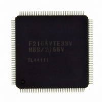
Manufacturer Part Number
DF2166VT33V
Description
IC H8S MCU FLASH 512K 144TQFP
Manufacturer
Renesas Electronics America
Series
H8® H8S/2100r
Specifications of DF2166VT33V
Core Processor
H8S/2000
Core Size
16-Bit
Speed
33MHz
Connectivity
I²C, IrDA, LPC, SCI, SmartCard
Peripherals
POR, PWM, WDT
Number Of I /o
106
Program Memory Size
512KB (512K x 8)
Program Memory Type
FLASH
Ram Size
40K x 8
Voltage - Supply (vcc/vdd)
3 V ~ 3.6 V
Data Converters
A/D 8x10b; D/A 2x8b
Oscillator Type
External
Operating Temperature
-20°C ~ 75°C
Package / Case
144-TQFP, 144-VQFP
Cpu Family
H8S
Device Core Size
16/32Bit
Frequency (max)
33MHz
Interface Type
I2C/IrDA/SCI
Total Internal Ram Size
40KB
# I/os (max)
106
Number Of Timers - General Purpose
5
Operating Supply Voltage (typ)
3.3V
Operating Supply Voltage (max)
3.6V
Operating Supply Voltage (min)
3V
On-chip Adc
8-chx10-bit
On-chip Dac
2-chx8-bit
Instruction Set Architecture
CISC
Operating Temp Range
-20C to 75C
Operating Temperature Classification
Commercial
Mounting
Surface Mount
Pin Count
144
Package Type
TQFP
Package
144TQFP
Family Name
H8S
Maximum Speed
33 MHz
Operating Supply Voltage
3.3 V
Data Bus Width
16|32 Bit
Number Of Programmable I/os
106
Number Of Timers
5
For Use With
HS0005KCU11H - EMULATOR E10A-USB H8S(X),SH2(A)3DK2166 - DEV EVAL KIT H8S/2166
Lead Free Status / RoHS Status
Lead free / RoHS Compliant
Eeprom Size
-
Lead Free Status / Rohs Status
Compliant
Other names
DF2166VTE33V
DF2166VTE33V
HD64F2166VTE33V
HD64F2166VTE33V
DF2166VTE33V
HD64F2166VTE33V
HD64F2166VTE33V
Available stocks
Company
Part Number
Manufacturer
Quantity
Price
Company:

Part Number:
DF2166VT33V
Manufacturer:
Exar
Quantity:
60
Company:
Part Number:
DF2166VT33V
Manufacturer:
Renesas Electronics America
Quantity:
10 000


20.6 Switching between User MAT and User Boot MAT........................................................ 668
20.7 Programmer Mode ............................................................................................................ 669
20.8 Serial Communication Interface Specification for Boot Mode......................................... 670
20.9 Usage Notes ...................................................................................................................... 695
Section 21 Boundary Scan (JTAG) ................................................................... 697
21.1 Features............................................................................................................................. 697
21.2 Input/Output Pins.............................................................................................................. 699
21.3 Register Descriptions........................................................................................................ 700
21.4 Operation .......................................................................................................................... 714
21.5 Boundary Scan.................................................................................................................. 715
21.6 Usage Notes ...................................................................................................................... 718
Section 22 Clock Pulse Generator..................................................................... 721
22.1 Oscillator........................................................................................................................... 722
22.2 PLL Multiplier Circuit ...................................................................................................... 724
22.3 Medium-Speed Clock Divider .......................................................................................... 724
22.4 Bus Master Clock Select Circuit....................................................................................... 724
22.5 Subclock Input Circuit ...................................................................................................... 724
22.6 Subclock Waveform Forming Circuit............................................................................... 724
22.7 Clock Select Circuit .......................................................................................................... 725
22.8 Usage Notes ...................................................................................................................... 725
Section 23 Power-Down Modes........................................................................ 727
23.1 Register Descriptions........................................................................................................ 728
Rev. 3.00, 03/04, page xxii of xl
20.5.1 Hardware Protection ............................................................................................ 665
20.5.2 Software Protection ............................................................................................. 666
20.5.3 Error Protection ................................................................................................... 666
21.3.1 Instruction Register (SDIR) ................................................................................. 701
21.3.2 Bypass Register (SDBPR) ................................................................................... 703
21.3.3 Boundary Scan Register (SDBSR) ...................................................................... 703
21.3.4 ID Code Register (SDIDR).................................................................................. 713
21.4.1 TAP Controller State Transitions......................................................................... 714
21.4.2 JTAG Reset.......................................................................................................... 715
21.5.1 Supported Instructions ......................................................................................... 715
22.1.1 Connecting Crystal Resonator ............................................................................. 722
22.1.2 External Clock Input Method .............................................................................. 723
22.8.1 Note on Resonator ............................................................................................... 725
22.8.2 Notes on Board Design ........................................................................................ 725
22.8.3 Note on Operation Check .................................................................................... 726
23.1.1 Standby Control Register (SBYCR) .................................................................... 728
23.1.2 Low-Power Control Register (LPWRCR) ........................................................... 730
Related parts for DF2166VT33V
Image
Part Number
Description
Manufacturer
Datasheet
Request
R

Part Number:
Description:
0.6mm Pitch Board-to-Fine-Coaxial Cable Connectors
Manufacturer:
Hirose Electric
Datasheet:
Part Number:
Description:
0.6mm Pitch Board-to-fine-coaxial Cable Connectors
Manufacturer:
Hirose Electric
Datasheet:
Part Number:
Description:
0.6mm Pitch Board-to-fine-coaxial Cable Connectors
Manufacturer:
Hirose Electric
Datasheet:
Part Number:
Description:
Right angle, Two-piece for fine coaxial cable, Discrete wire connectors; HRS No: 687-0001-5 56; No. of Positions: 20; Connector Type: Board mounting; Contact Gender: Female; Contact Spacing (mm): 0.6; Terminal Pitch (mm): 0.6; PCB Mount Type: SMT; Cu
Manufacturer:
Hirose Electric
Part Number:
Description:
0.6mm Pitch Board-to-fine-coaxial Cable Connectors
Manufacturer:
Hirose Electric
Datasheet:
Part Number:
Description:
0.6mm Pitch Board-to-Fine-Coaxial Cable Connectors
Manufacturer:
HIROSE [Hirose Electric]
Datasheet:

Part Number:
Description:
KIT STARTER FOR M16C/29
Manufacturer:
Renesas Electronics America
Datasheet:

Part Number:
Description:
KIT STARTER FOR R8C/2D
Manufacturer:
Renesas Electronics America
Datasheet:

Part Number:
Description:
R0K33062P STARTER KIT
Manufacturer:
Renesas Electronics America
Datasheet:

Part Number:
Description:
KIT STARTER FOR R8C/23 E8A
Manufacturer:
Renesas Electronics America
Datasheet:

Part Number:
Description:
KIT STARTER FOR R8C/25
Manufacturer:
Renesas Electronics America
Datasheet:

Part Number:
Description:
KIT STARTER H8S2456 SHARPE DSPLY
Manufacturer:
Renesas Electronics America
Datasheet:

Part Number:
Description:
KIT STARTER FOR R8C38C
Manufacturer:
Renesas Electronics America
Datasheet:

Part Number:
Description:
KIT STARTER FOR R8C35C
Manufacturer:
Renesas Electronics America
Datasheet:

Part Number:
Description:
KIT STARTER FOR R8CL3AC+LCD APPS
Manufacturer:
Renesas Electronics America
Datasheet: