DF2166VT33V Renesas Electronics America, DF2166VT33V Datasheet - Page 42
DF2166VT33V
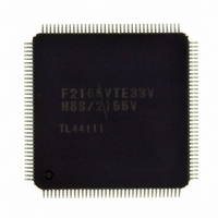
Manufacturer Part Number
DF2166VT33V
Description
IC H8S MCU FLASH 512K 144TQFP
Manufacturer
Renesas Electronics America
Series
H8® H8S/2100r
Specifications of DF2166VT33V
Core Processor
H8S/2000
Core Size
16-Bit
Speed
33MHz
Connectivity
I²C, IrDA, LPC, SCI, SmartCard
Peripherals
POR, PWM, WDT
Number Of I /o
106
Program Memory Size
512KB (512K x 8)
Program Memory Type
FLASH
Ram Size
40K x 8
Voltage - Supply (vcc/vdd)
3 V ~ 3.6 V
Data Converters
A/D 8x10b; D/A 2x8b
Oscillator Type
External
Operating Temperature
-20°C ~ 75°C
Package / Case
144-TQFP, 144-VQFP
Cpu Family
H8S
Device Core Size
16/32Bit
Frequency (max)
33MHz
Interface Type
I2C/IrDA/SCI
Total Internal Ram Size
40KB
# I/os (max)
106
Number Of Timers - General Purpose
5
Operating Supply Voltage (typ)
3.3V
Operating Supply Voltage (max)
3.6V
Operating Supply Voltage (min)
3V
On-chip Adc
8-chx10-bit
On-chip Dac
2-chx8-bit
Instruction Set Architecture
CISC
Operating Temp Range
-20C to 75C
Operating Temperature Classification
Commercial
Mounting
Surface Mount
Pin Count
144
Package Type
TQFP
Package
144TQFP
Family Name
H8S
Maximum Speed
33 MHz
Operating Supply Voltage
3.3 V
Data Bus Width
16|32 Bit
Number Of Programmable I/os
106
Number Of Timers
5
For Use With
HS0005KCU11H - EMULATOR E10A-USB H8S(X),SH2(A)3DK2166 - DEV EVAL KIT H8S/2166
Lead Free Status / RoHS Status
Lead free / RoHS Compliant
Eeprom Size
-
Lead Free Status / Rohs Status
Compliant
Other names
DF2166VTE33V
DF2166VTE33V
HD64F2166VTE33V
HD64F2166VTE33V
DF2166VTE33V
HD64F2166VTE33V
HD64F2166VTE33V
Available stocks
Company
Part Number
Manufacturer
Quantity
Price
Company:

Part Number:
DF2166VT33V
Manufacturer:
Exar
Quantity:
60
Company:
Part Number:
DF2166VT33V
Manufacturer:
Renesas Electronics America
Quantity:
10 000


Section 23 Power-Down Modes
Table 23.1
Table 23.2
Section 25 Electrical Characteristics
Table 25.1
Table 25.2
Table 25.2
Table 25.3
Table 25.4
Table 25.5
Table 25.6
Table 25.7
Table 25.8
Table 25.9
Table 25.10
Table 25.11
Table 25.12
Table 25.13
Table 25.14
Table 25.15
Table 25.16
Rev. 3.00, 03/04, page xl of xl
Operating Frequency and Wait Time.................................................................... 730
LSI Internal States in Each Mode ......................................................................... 737
Absolute Maximum Ratings ................................................................................. 783
DC Characteristics (1) .......................................................................................... 784
DC Characteristics (2) .......................................................................................... 785
Permissible Output Currents................................................................................. 787
Clock Timing ........................................................................................................ 788
External Clock Input Conditions .......................................................................... 789
Subclock Input Conditions.................................................................................... 789
Control Signal Timing .......................................................................................... 792
Bus Timing ........................................................................................................... 794
Multiplex Bus Timing........................................................................................... 800
Timing of On-Chip Peripheral Modules ........................................................... 803
I
LPC Module Timing......................................................................................... 808
JTAG Timing.................................................................................................... 809
A/D Conversion Characteristics
D/A Conversion Characteristics ....................................................................... 812
Flash Memory Characteristics .......................................................................... 813
(AN7 to AN0 Input: 134/266-State Conversion).............................................. 811
2
C Bus Timing ................................................................................................. 807
Related parts for DF2166VT33V
Image
Part Number
Description
Manufacturer
Datasheet
Request
R

Part Number:
Description:
0.6mm Pitch Board-to-Fine-Coaxial Cable Connectors
Manufacturer:
Hirose Electric
Datasheet:
Part Number:
Description:
0.6mm Pitch Board-to-fine-coaxial Cable Connectors
Manufacturer:
Hirose Electric
Datasheet:
Part Number:
Description:
0.6mm Pitch Board-to-fine-coaxial Cable Connectors
Manufacturer:
Hirose Electric
Datasheet:
Part Number:
Description:
Right angle, Two-piece for fine coaxial cable, Discrete wire connectors; HRS No: 687-0001-5 56; No. of Positions: 20; Connector Type: Board mounting; Contact Gender: Female; Contact Spacing (mm): 0.6; Terminal Pitch (mm): 0.6; PCB Mount Type: SMT; Cu
Manufacturer:
Hirose Electric
Part Number:
Description:
0.6mm Pitch Board-to-fine-coaxial Cable Connectors
Manufacturer:
Hirose Electric
Datasheet:
Part Number:
Description:
0.6mm Pitch Board-to-Fine-Coaxial Cable Connectors
Manufacturer:
HIROSE [Hirose Electric]
Datasheet:

Part Number:
Description:
KIT STARTER FOR M16C/29
Manufacturer:
Renesas Electronics America
Datasheet:

Part Number:
Description:
KIT STARTER FOR R8C/2D
Manufacturer:
Renesas Electronics America
Datasheet:

Part Number:
Description:
R0K33062P STARTER KIT
Manufacturer:
Renesas Electronics America
Datasheet:

Part Number:
Description:
KIT STARTER FOR R8C/23 E8A
Manufacturer:
Renesas Electronics America
Datasheet:

Part Number:
Description:
KIT STARTER FOR R8C/25
Manufacturer:
Renesas Electronics America
Datasheet:

Part Number:
Description:
KIT STARTER H8S2456 SHARPE DSPLY
Manufacturer:
Renesas Electronics America
Datasheet:

Part Number:
Description:
KIT STARTER FOR R8C38C
Manufacturer:
Renesas Electronics America
Datasheet:

Part Number:
Description:
KIT STARTER FOR R8C35C
Manufacturer:
Renesas Electronics America
Datasheet:

Part Number:
Description:
KIT STARTER FOR R8CL3AC+LCD APPS
Manufacturer:
Renesas Electronics America
Datasheet: