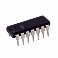
PIC16F684-E/P Microchip Technology, PIC16F684-E/P Datasheet - Page 148

PIC16F684-E/P
Manufacturer Part Number
PIC16F684-E/P
Description
IC PIC MCU FLASH 2KX14 14DIP
Manufacturer
Microchip Technology
Series
PIC® 16Fr
Datasheets
1.PIC16F616T-ISL.pdf
(8 pages)
2.PIC16F688T-ISL.pdf
(688 pages)
3.PIC16F684-ISL.pdf
(4 pages)
4.PIC16F684-ISL.pdf
(192 pages)
5.PIC16F684-ISL.pdf
(6 pages)
6.PIC16F684-IST.pdf
(164 pages)
Specifications of PIC16F684-E/P
Program Memory Type
FLASH
Program Memory Size
3.5KB (2K x 14)
Package / Case
14-DIP (0.300", 7.62mm)
Core Processor
PIC
Core Size
8-Bit
Speed
20MHz
Peripherals
Brown-out Detect/Reset, POR, PWM, WDT
Number Of I /o
12
Eeprom Size
256 x 8
Ram Size
128 x 8
Voltage - Supply (vcc/vdd)
2 V ~ 5.5 V
Data Converters
A/D 8x10b
Oscillator Type
Internal
Operating Temperature
-40°C ~ 125°C
Processor Series
PIC16F
Core
PIC
Data Bus Width
8 bit
Data Ram Size
128 B
Maximum Clock Frequency
20 MHz
Number Of Programmable I/os
12
Number Of Timers
3
Operating Supply Voltage
2 V to 5.5 V
Maximum Operating Temperature
+ 125 C
Mounting Style
Through Hole
3rd Party Development Tools
52715-96, 52716-328, 52717-734
Development Tools By Supplier
PG164130, DV164035, DV244005, DV164005, PG164120, ICE2000, DM163014, DM164120-4
Minimum Operating Temperature
- 40 C
On-chip Adc
8-ch x 10-bit
Lead Free Status / RoHS Status
Lead free / RoHS Compliant
For Use With
DM163029 - BOARD PICDEM FOR MECHATRONICSACICE0207 - MPLABICE 14P 300 MIL ADAPTER
Connectivity
-
Lead Free Status / Rohs Status
Lead free / RoHS Compliant
PIC16F684
FIGURE 15-10:
TABLE 15-11: PIC16F684 A/D CONVERSION REQUIREMENTS (SLEEP MODE)
DS41202C-page 146
Standard Operating Conditions (unless otherwise stated)
Operating temperature
130
131
132
134
Note 1:
Param
No.
Note 1: If the A/D clock source is selected as RC, a time of T
A/D Data
A/D CLK
2:
BSF ADCON0, GO
ADRES
Sample
*
† Data in ‘Typ’ column is at 5.0V, 25 C unless otherwise stated. These parameters are for design guidance
ADIF
GO
These parameters are characterized but not tested.
only and are not tested.
ADRES register may be read on the following T
See Table 9-1 for minimum conditions.
T
T
T
T
Q4
CNV
ACQ
AD
GO
Sym
SLEEP instruction to be executed.
134
132
A/D Internal RC
Oscillator Period
Conversion Time
(not including
Acquisition Time)
Acquisition Time
Q4 to A/D Clock
Start
PIC16F684 A/D CONVERSION TIMING (SLEEP MODE)
Characteristic
-40°C
(T
OSC
T
/2 + T
A
(1)
+125°C
CY
9
)
(1)
2.0*
Min
3.0*
(2)
—
—
5*
OLD_DATA
Sampling Stopped
8
Preliminary
T
OSC
7
Typ†
11.5
131
6.0
4.0
/2 + T
11
—
CY
cycle.
6
CY
CY
130
is added before the A/D clock starts. This allows the
Max
9.0*
6.0*
3
—
—
—
—
Units
2
T
—
AD
s
s
s
s
1
ADCS<1:0> = 11 (RC mode)
At V
At V
The minimum time is the amplifier
settling time. This may be used if
the “new” input voltage has not
changed by more than 1 LSb (i.e.,
4.1 mV @ 4.096V) from the last
sampled voltage (as stored on
C
If the A/D clock source is selected
as RC, a time of T
before the A/D clock starts. This
allows the SLEEP instruction to be
executed.
HOLD
2004 Microchip Technology Inc.
DD
DD
0
).
= 2.5V
= 5.0V
NEW_DATA
Conditions
1 T
DONE
CY
1 T
CY
CY
is added


