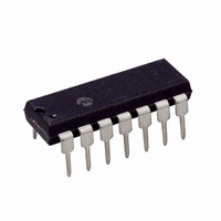
PIC16F684-E/P Microchip Technology, PIC16F684-E/P Datasheet - Page 38

PIC16F684-E/P
Manufacturer Part Number
PIC16F684-E/P
Description
IC PIC MCU FLASH 2KX14 14DIP
Manufacturer
Microchip Technology
Series
PIC® 16Fr
Datasheets
1.PIC16F616T-ISL.pdf
(8 pages)
2.PIC16F688T-ISL.pdf
(688 pages)
3.PIC16F684-ISL.pdf
(4 pages)
4.PIC16F684-ISL.pdf
(192 pages)
5.PIC16F684-ISL.pdf
(6 pages)
6.PIC16F684-IST.pdf
(164 pages)
Specifications of PIC16F684-E/P
Program Memory Type
FLASH
Program Memory Size
3.5KB (2K x 14)
Package / Case
14-DIP (0.300", 7.62mm)
Core Processor
PIC
Core Size
8-Bit
Speed
20MHz
Peripherals
Brown-out Detect/Reset, POR, PWM, WDT
Number Of I /o
12
Eeprom Size
256 x 8
Ram Size
128 x 8
Voltage - Supply (vcc/vdd)
2 V ~ 5.5 V
Data Converters
A/D 8x10b
Oscillator Type
Internal
Operating Temperature
-40°C ~ 125°C
Processor Series
PIC16F
Core
PIC
Data Bus Width
8 bit
Data Ram Size
128 B
Maximum Clock Frequency
20 MHz
Number Of Programmable I/os
12
Number Of Timers
3
Operating Supply Voltage
2 V to 5.5 V
Maximum Operating Temperature
+ 125 C
Mounting Style
Through Hole
3rd Party Development Tools
52715-96, 52716-328, 52717-734
Development Tools By Supplier
PG164130, DV164035, DV244005, DV164005, PG164120, ICE2000, DM163014, DM164120-4
Minimum Operating Temperature
- 40 C
On-chip Adc
8-ch x 10-bit
Lead Free Status / RoHS Status
Lead free / RoHS Compliant
For Use With
DM163029 - BOARD PICDEM FOR MECHATRONICSACICE0207 - MPLABICE 14P 300 MIL ADAPTER
Connectivity
-
Lead Free Status / Rohs Status
Lead free / RoHS Compliant
PIC16F684
4.2.4
Each PORTA pin is multiplexed with other functions.
The pins and their combined functions are briefly
described here. For specific information about individ-
ual functions such as the comparator or the A/D, refer
to the appropriate section in this data sheet.
4.2.4.1
Figure 4-2 shows the diagram for this pin. The RA0 pin
is configurable to function as one of the following:
• a general purpose I/O
• an analog input for the A/D
• an analog input to the comparator
• In-Circuit Serial Programming data
• an analog input for the Ultra Low-power Wake-up
4.2.4.2
Figure 4-2 shows the diagram for this pin. The RA1 pin
is configurable to function as one of the following:
• a general purpose I/O
• an analog input for the A/D
• an analog input to the comparator
• a voltage reference input for the A/D
• In-Circuit Serial Programming clock
DS41202C-page 36
PIN DESCRIPTIONS AND
DIAGRAMS
RA0/AN0/C1IN+/ICSPDAT/ULPWU
RA1/AN1/C1IN-/V
REF
/ICSPCLK
Preliminary
FIGURE 4-2:
Data Bus
PORTA
PORTA
WPUA
WPUA
TRISA
TRISA
IOCA
IOCA
Interrupt-on-
Note 1:
WR
WR
WR
WR
RD
RD
RD
RD
Change
D
D
D
D
CK
CK
CK
CK
To Comparator
To A/D Converter
Comparator mode and ANSEL determines Analog
Input mode.
Q
Q
Q
Q
Q
Q
Q
Q
Input Mode
BLOCK DIAGRAM OF RA1
Analog
RD PORTA
2004 Microchip Technology Inc.
Input Mode
(1)
RAPU
Analog
Q
Q
(1)
EN
EN
D
D
V
DD
Weak
V
V
DD
Q3
SS
I/O PIN


