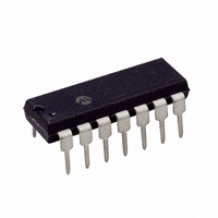
PIC16F684-E/P Microchip Technology, PIC16F684-E/P Datasheet - Page 9

PIC16F684-E/P
Manufacturer Part Number
PIC16F684-E/P
Description
IC PIC MCU FLASH 2KX14 14DIP
Manufacturer
Microchip Technology
Series
PIC® 16Fr
Datasheets
1.PIC16F616T-ISL.pdf
(8 pages)
2.PIC16F688T-ISL.pdf
(688 pages)
3.PIC16F684-ISL.pdf
(4 pages)
4.PIC16F684-ISL.pdf
(192 pages)
5.PIC16F684-ISL.pdf
(6 pages)
6.PIC16F684-IST.pdf
(164 pages)
Specifications of PIC16F684-E/P
Program Memory Type
FLASH
Program Memory Size
3.5KB (2K x 14)
Package / Case
14-DIP (0.300", 7.62mm)
Core Processor
PIC
Core Size
8-Bit
Speed
20MHz
Peripherals
Brown-out Detect/Reset, POR, PWM, WDT
Number Of I /o
12
Eeprom Size
256 x 8
Ram Size
128 x 8
Voltage - Supply (vcc/vdd)
2 V ~ 5.5 V
Data Converters
A/D 8x10b
Oscillator Type
Internal
Operating Temperature
-40°C ~ 125°C
Processor Series
PIC16F
Core
PIC
Data Bus Width
8 bit
Data Ram Size
128 B
Maximum Clock Frequency
20 MHz
Number Of Programmable I/os
12
Number Of Timers
3
Operating Supply Voltage
2 V to 5.5 V
Maximum Operating Temperature
+ 125 C
Mounting Style
Through Hole
3rd Party Development Tools
52715-96, 52716-328, 52717-734
Development Tools By Supplier
PG164130, DV164035, DV244005, DV164005, PG164120, ICE2000, DM163014, DM164120-4
Minimum Operating Temperature
- 40 C
On-chip Adc
8-ch x 10-bit
Lead Free Status / RoHS Status
Lead free / RoHS Compliant
For Use With
DM163029 - BOARD PICDEM FOR MECHATRONICSACICE0207 - MPLABICE 14P 300 MIL ADAPTER
Connectivity
-
Lead Free Status / Rohs Status
Lead free / RoHS Compliant
2.0
2.1
The PIC16F684 has a 13-bit program counter capable
of addressing an 8k x 14 program memory space. Only
the first 2k x 14 (0000h-07FFh) for the PIC16F684 is
physically implemented. Accessing a location above
these boundaries will cause a wrap around within the
first 2k x 14 space. The Reset vector is at 0000h and
the interrupt vector is at 0004h (see Figure 2-1).
FIGURE 2-1:
2004 Microchip Technology Inc.
CALL, RETURN
RETFIE, RETLW
MEMORY ORGANIZATION
Program Memory Organization
On-chip Program
Interrupt Vector
Stack Level 1
Stack Level 2
Stack Level 8
Reset Vector
PC<12:0>
Memory
PROGRAM MEMORY MAP
AND STACK FOR THE
PIC16F684
13
000h
0004
0005
07FFh
0800h
1FFFh
Preliminary
2.2
The data memory (see Figure 2-2) is partitioned into
two banks, which contain the General Purpose Regis-
ters (GPR) and the Special Function Registers (SFR).
The Special Function Registers are located in the first
32 locations of each bank. Register locations 20h-7Fh
in Bank 0 and A0h-BFh in Bank 1 are General Purpose
Registers, implemented as static RAM. Register
locations F0h-FFh in Bank 1 point to addresses
70h-7Fh in Bank 0. All other RAM is unimplemented
and returns ‘0’ when read. RP0 (Status<5>) is the bank
select bit.
RP0 = 0:
RP0 = 1:
Note:
Data Memory Organization
The IRP and RP1 bits Status<7:6> are
reserved
maintained as ‘0’s.
Bank 0 is selected
Bank 1 is selected
and
PIC16F684
should
DS41202C-page 7
always
be


