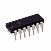
PIC16F684-E/P Microchip Technology, PIC16F684-E/P Datasheet - Page 66

PIC16F684-E/P
Manufacturer Part Number
PIC16F684-E/P
Description
IC PIC MCU FLASH 2KX14 14DIP
Manufacturer
Microchip Technology
Series
PIC® 16Fr
Datasheets
1.PIC16F616T-ISL.pdf
(8 pages)
2.PIC16F688T-ISL.pdf
(688 pages)
3.PIC16F684-ISL.pdf
(4 pages)
4.PIC16F684-ISL.pdf
(192 pages)
5.PIC16F684-ISL.pdf
(6 pages)
6.PIC16F684-IST.pdf
(164 pages)
Specifications of PIC16F684-E/P
Program Memory Type
FLASH
Program Memory Size
3.5KB (2K x 14)
Package / Case
14-DIP (0.300", 7.62mm)
Core Processor
PIC
Core Size
8-Bit
Speed
20MHz
Peripherals
Brown-out Detect/Reset, POR, PWM, WDT
Number Of I /o
12
Eeprom Size
256 x 8
Ram Size
128 x 8
Voltage - Supply (vcc/vdd)
2 V ~ 5.5 V
Data Converters
A/D 8x10b
Oscillator Type
Internal
Operating Temperature
-40°C ~ 125°C
Processor Series
PIC16F
Core
PIC
Data Bus Width
8 bit
Data Ram Size
128 B
Maximum Clock Frequency
20 MHz
Number Of Programmable I/os
12
Number Of Timers
3
Operating Supply Voltage
2 V to 5.5 V
Maximum Operating Temperature
+ 125 C
Mounting Style
Through Hole
3rd Party Development Tools
52715-96, 52716-328, 52717-734
Development Tools By Supplier
PG164130, DV164035, DV244005, DV164005, PG164120, ICE2000, DM163014, DM164120-4
Minimum Operating Temperature
- 40 C
On-chip Adc
8-ch x 10-bit
Lead Free Status / RoHS Status
Lead free / RoHS Compliant
For Use With
DM163029 - BOARD PICDEM FOR MECHATRONICSACICE0207 - MPLABICE 14P 300 MIL ADAPTER
Connectivity
-
Lead Free Status / Rohs Status
Lead free / RoHS Compliant
PIC16F684
9.1.4
The A/D conversion cycle requires 11 T
of the conversion clock is software selectable via the
ADCS bits (ADCON1<6:4>). There are seven possible
clock options:
• F
• F
• F
TABLE 9-1:
9.1.5
The A/D conversion is initiated by setting the
GO/DONE bit (ADCON0<1>). When the conversion is
complete, the A/D module:
• Clears the GO/DONE bit
• Sets the ADIF flag (PIR1<6>)
• Generates an interrupt (if enabled)
FIGURE 9-2:
DS41202C-page 64
Legend: Shaded cells are outside of recommended range.
Note 1:
Operation
OSC
OSC
OSC
16 T
32 T
64 T
A/D RC
2 T
4 T
8 T
A/D Clock Source (T
2:
3:
4:
/2
/4
/8
OSC
OSC
OSC
OSC
OSC
OSC
The A/D RC source has a typical T
These values violate the minimum required T
For faster conversion times, the selection of another clock source is recommended.
When the device frequency is greater than 1 MHz, the A/D RC clock source is only recommended if the
conversion will be performed during Sleep.
CONVERSION CLOCK
STARTING A CONVERSION
T
CY
Set GO bit
Holding Capacitor is Disconnected from Analog Input (typically 100 ns)
to T
ADCS2:ADCS0
T
AD
AD
Conversion Starts
A/D CONVERSION T
VS. DEVICE OPERATING FREQUENCIES
T
000
100
001
101
010
110
x11
AD
1
AD
)
T
AD
b9
2
T
AD
b8
AD
3
2-6 s
. The source
100 ns
200 ns
400 ns
800 ns
20 MHz
1.6 s
3.2 s
T
AD
b7
AD
AD
4
(1,4)
(2)
(2)
(2)
(2)
time of 4 s for V
CYCLES
T
Preliminary
AD
b6
5
AD
T
AD
b5
time.
6
2-6 s
12.8 s
400 ns
800 ns
• F
• F
• F
• F
For correct conversion, the A/D conversion clock
(1/T
1.6 s. Table 9-1 shows a few T
selected frequencies.
If the conversion must be aborted, the GO/DONE bit
can be cleared in software. The ADRESH:ADRESL
registers will not be updated with the partially complete
A/D
ADRESH:ADRESL registers will retain the value of the
previous conversion. After an aborted conversion, a
2 T
be initiated. Following the delay, an input acquisition is
automatically started on the selected channel.
5 MHz
ADRESH and ADRESL registers are Loaded,
GO bit is Cleared,
ADIF bit is Set,
Holding Capacitor is Connected to Analog Input
1.6 s
3.2 s
6.4 s
T
AD
b4
Note:
AD
DD
7
OSC
OSC
OSC
RC
AD
Device Frequency
(1,4)
(2)
(2)
(3)
) must be selected to ensure a minimum T
> 3.0V.
delay is required before another acquisition can
(dedicated internal oscillator)
T
/16
/32
/64
AD
b3
conversion
8
The GO/DONE bit should not be set in the
same instruction that turns on the A/D.
T
AD
b2
9
2-6 s
16.0 s
500 ns
1.0 s
8.0 s
T
4 MHz
AD
2.0 s
4.0 s
b1
10 T
2004 Microchip Technology Inc.
sample.
(1,4)
(2)
(3)
(2)
(3)
AD
b0
11
AD
Instead,
calculations for
2-6 s
1.25 MHz
12.8 s
25.6 s
51.2 s
1.6 s
3.2 s
6.4 s
(1,4)
(3)
(3)
(3)
AD
the
of


