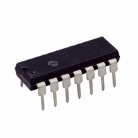
PIC16F684-E/P Microchip Technology, PIC16F684-E/P Datasheet - Page 90

PIC16F684-E/P
Manufacturer Part Number
PIC16F684-E/P
Description
IC PIC MCU FLASH 2KX14 14DIP
Manufacturer
Microchip Technology
Series
PIC® 16Fr
Datasheets
1.PIC16F616T-ISL.pdf
(8 pages)
2.PIC16F688T-ISL.pdf
(688 pages)
3.PIC16F684-ISL.pdf
(4 pages)
4.PIC16F684-ISL.pdf
(192 pages)
5.PIC16F684-ISL.pdf
(6 pages)
6.PIC16F684-IST.pdf
(164 pages)
Specifications of PIC16F684-E/P
Program Memory Type
FLASH
Program Memory Size
3.5KB (2K x 14)
Package / Case
14-DIP (0.300", 7.62mm)
Core Processor
PIC
Core Size
8-Bit
Speed
20MHz
Peripherals
Brown-out Detect/Reset, POR, PWM, WDT
Number Of I /o
12
Eeprom Size
256 x 8
Ram Size
128 x 8
Voltage - Supply (vcc/vdd)
2 V ~ 5.5 V
Data Converters
A/D 8x10b
Oscillator Type
Internal
Operating Temperature
-40°C ~ 125°C
Processor Series
PIC16F
Core
PIC
Data Bus Width
8 bit
Data Ram Size
128 B
Maximum Clock Frequency
20 MHz
Number Of Programmable I/os
12
Number Of Timers
3
Operating Supply Voltage
2 V to 5.5 V
Maximum Operating Temperature
+ 125 C
Mounting Style
Through Hole
3rd Party Development Tools
52715-96, 52716-328, 52717-734
Development Tools By Supplier
PG164130, DV164035, DV244005, DV164005, PG164120, ICE2000, DM163014, DM164120-4
Minimum Operating Temperature
- 40 C
On-chip Adc
8-ch x 10-bit
Lead Free Status / RoHS Status
Lead free / RoHS Compliant
For Use With
DM163029 - BOARD PICDEM FOR MECHATRONICSACICE0207 - MPLABICE 14P 300 MIL ADAPTER
Connectivity
-
Lead Free Status / Rohs Status
Lead free / RoHS Compliant
PIC16F684
11.3.9
In Sleep mode, all clock sources are disabled. Timer2
will not increment, and the state of the module will not
change. If the ECCP pin is driving a value, it will
continue to drive that value. When the device wakes
up, it will continue from this state.
11.3.9.1
If the Fail-Safe Clock Monitor is enabled, a clock failure
will force the ECCP to be clocked from the internal
oscillator clock source, which may have a different
clock frequency than the primary clock.
See Section 3.0 “Clock Sources” for additional
details.
11.3.10
Any Reset will force all ports to Input mode and the
ECCP registers to their Reset states.
This forces the Enhanced CCP module to reset to a
state compatible with the standard CCP module.
DS41202C-page 88
OPERATION IN SLEEP MODE
EFFECTS OF A RESET
OPERATION WITH FAIL-SAFE
CLOCK MONITOR
Preliminary
11.3.11
The following steps should be taken when configuring
the ECCP module for PWM operation:
1.
2.
3.
4.
5.
6.
7.
8.
9.
Configure the PWM pins P1A and P1B (and
P1C and P1D, if used) as inputs by setting the
corresponding TRISC bits.
Set the PWM period by loading the PR2 register.
Configure the ECCP module for the desired
PWM mode and configuration by loading the
CCP1CON register with the appropriate values:
• Select one of the available output
• Select the polarities of the PWM output
Set the PWM duty cycle by loading the CCPR1L
register and CCP1CON<5:4> bits.
For Half-bridge Output mode, set the dead band
delay by loading PWM1CON<6:0> with the
appropriate value.
If auto-shutdown operation is required, load the
ECCPAS register:
• Select the auto-shutdown sources using the
• Select the shutdown states of the PWM
• Set the ECCPASE bit (ECCPAS<7>).
• Configure the comparators using the
• Configure the comparator inputs as analog
If auto-restart operation is required, set the
PRSEN bit (PWM1CON<7>).
Configure and start TMR2:
• Clear the TMR2 interrupt flag bit by clearing
• Set the TMR2 prescale value by loading the
• Enable Timer2 by setting the TMR2ON bit
Enable PWM outputs after a new PWM cycle
has started:
• Wait until TMR2 overflows (TMR2IF bit is set).
• Enable the CCP1/P1A, P1B, P1C and/or P1D
• Clear the ECCPASE bit (ECCPAS<7>).
configurations and direction with the
P1M<1:0> bits.
signals with the CCP1M<3:0> bits.
ECCPAS<2:0> bits.
output pins using PSSAC<1:0> and
PSSBD<1:0> bits.
CMCON0 register (Register 8-1).
inputs.
the TMR2IF bit (PIR1<1>).
T2CKPS bits (T2CON<1:0>).
(T2CON<2>).
pin outputs by clearing the respective TRISC
bits.
SETUP FOR PWM OPERATION
2004 Microchip Technology Inc.


