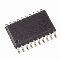
AT90PWM81-16SN Atmel, AT90PWM81-16SN Datasheet - Page 136

AT90PWM81-16SN
Manufacturer Part Number
AT90PWM81-16SN
Description
IC MCU AVR 8K FLASH ISP 20SOIC
Manufacturer
Atmel
Series
AVR® 90PWM Lightingr
Datasheet
1.AT90PWM81-16MN.pdf
(325 pages)
Specifications of AT90PWM81-16SN
Core Processor
AVR
Core Size
8-Bit
Speed
16MHz
Connectivity
SPI
Peripherals
Brown-out Detect/Reset, PWM, WDT
Number Of I /o
16
Program Memory Size
8KB (8K x 8)
Program Memory Type
FLASH
Eeprom Size
512 x 8
Ram Size
256 x 8
Voltage - Supply (vcc/vdd)
2.7 V ~ 5.5 V
Data Converters
A/D 8x10b; D/A 1x10b
Oscillator Type
Internal
Operating Temperature
-40°C ~ 105°C
Package / Case
20-SOIC (7.5mm Width)
Data Bus Width
8 bit
Data Ram Size
256 B
Interface Type
SPI
Maximum Clock Frequency
16 MHz
Number Of Timers
1
Maximum Operating Temperature
+ 105 C
Mounting Style
SMD/SMT
Minimum Operating Temperature
- 40 C
On-chip Adc
10 bit, 8 Channel
On-chip Dac
10 bit, 1 Channel
Height
2.35 mm
Length
13 mm
Supply Voltage (max)
5.5 V
Supply Voltage (min)
2.7 V
Width
7.6 mm
For Use With
ATSTK600-SOIC - STK600 SOCKET/ADAPTER FOR SOIC
Lead Free Status / RoHS Status
Lead free / RoHS Compliant
Available stocks
Company
Part Number
Manufacturer
Quantity
Price
Company:
Part Number:
AT90PWM81-16SN
Manufacturer:
Atmel
Quantity:
1 500
- Current page: 136 of 325
- Download datasheet (6Mb)
12.25.7
Table 12-14.
136
PASDLKn2
0
0
0
0
AT90PWM81
PSC 2 Extended Configuration Register – PCNFE2
Analog signal synchronization or Input Blanking Mode Selection
PASDLKn1
0
0
1
1
• Bit 4:3 – PMODEn1: 0: PSC n Mode
Select the mode of PSC.
Table 12-13.
• Bit 2 – POPn: PSC n Output Polarity
If this bit is cleared, the PSC outputs are active Low.
If this bit is set, the PSC outputs are active High.
• Bit 1 – PCLKSELn: PSC n Input Clock Select
This bit is used to select between CLKPF or CLKPS clocks.
Set this bit to select the fast clock input (CLKPF).
Clear this bit to select the slow clock input (CLKPS).
• Bit 0 – POME2: PSC 2 Output Matrix Enable (PSC2 only)
Set this bit to enable the Output Matrix feature on PSC2 outputs. See
When Output Matrix is used, the PSC n Output Polarity POPn has no action on the outputs.
The PSC n Extended Configuration Register is used to configure the running mode of the PSC
• Bit 7, 6, 5– PASDLKn(2:0): Analog Synchronization Output Delay or Input Blanking select
Defines the modes for Analog signal synchronization delay or Input Blanking.
Bit
Read/Write
Initial Value
PMODEn1
0
0
1
1
PASDLKn0
0
1
0
1
7
PASDLKn2 PASDLKn1 PASDLKn0 PBFMn1
R/W
0
PSC n Mode Selection
PMODEn0
0
1
0
1
6
R/W
0
Description
No Analog signal synchronization delay, no Input Blanking
No Analog signal synchronization delay , Input Blanking using PSC clock, started
on PSC end of cycle
No Analog signal synchronization delay , Input Blanking using PSC clock, started
on OCR SA event
No Analog signal synchronization delay , Input Blanking using PSC clock, started
on OCR SB event
5
R/W
0
One Ramp Mode
Two Ramp Mode
Four Ramp Mode
Center Aligned Mode
Description
4
R/W
0
3
PELEVnA1 PELEVnB1 PISELnA1 PISELnB1 PCNFE2
0
R/W
2
R/W
0
“PSC2 Outputs” on page
1
R/W
0
0
R/W
0
7734P–AVR–08/10
129.
Related parts for AT90PWM81-16SN
Image
Part Number
Description
Manufacturer
Datasheet
Request
R

Part Number:
Description:
Manufacturer:
Atmel Corporation
Datasheet:

Part Number:
Description:
IC MCU AVR 8K FLASH ISP 32QFN
Manufacturer:
Atmel
Datasheet:

Part Number:
Description:
IC MCU AVR 8K FLASH ISP 32QFN
Manufacturer:
Atmel
Datasheet:

Part Number:
Description:
IC MCU AVR 8K FLASH ISP 20SOIC
Manufacturer:
Atmel
Datasheet:

Part Number:
Description:
8-bit Avr Microcontroller With 8k Bytes In- System Programmable Flash
Manufacturer:
ATMEL Corporation
Datasheet:

Part Number:
Description:
DEV KIT FOR AVR/AVR32
Manufacturer:
Atmel
Datasheet:

Part Number:
Description:
INTERVAL AND WIPE/WASH WIPER CONTROL IC WITH DELAY
Manufacturer:
ATMEL Corporation
Datasheet:

Part Number:
Description:
Low-Voltage Voice-Switched IC for Hands-Free Operation
Manufacturer:
ATMEL Corporation
Datasheet:

Part Number:
Description:
MONOLITHIC INTEGRATED FEATUREPHONE CIRCUIT
Manufacturer:
ATMEL Corporation
Datasheet:

Part Number:
Description:
AM-FM Receiver IC U4255BM-M
Manufacturer:
ATMEL Corporation
Datasheet:

Part Number:
Description:
Monolithic Integrated Feature Phone Circuit
Manufacturer:
ATMEL Corporation
Datasheet:

Part Number:
Description:
Multistandard Video-IF and Quasi Parallel Sound Processing
Manufacturer:
ATMEL Corporation
Datasheet:


