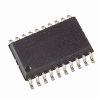
AT90PWM81-16SN Atmel, AT90PWM81-16SN Datasheet - Page 92

AT90PWM81-16SN
Manufacturer Part Number
AT90PWM81-16SN
Description
IC MCU AVR 8K FLASH ISP 20SOIC
Manufacturer
Atmel
Series
AVR® 90PWM Lightingr
Datasheet
1.AT90PWM81-16MN.pdf
(325 pages)
Specifications of AT90PWM81-16SN
Core Processor
AVR
Core Size
8-Bit
Speed
16MHz
Connectivity
SPI
Peripherals
Brown-out Detect/Reset, PWM, WDT
Number Of I /o
16
Program Memory Size
8KB (8K x 8)
Program Memory Type
FLASH
Eeprom Size
512 x 8
Ram Size
256 x 8
Voltage - Supply (vcc/vdd)
2.7 V ~ 5.5 V
Data Converters
A/D 8x10b; D/A 1x10b
Oscillator Type
Internal
Operating Temperature
-40°C ~ 105°C
Package / Case
20-SOIC (7.5mm Width)
Data Bus Width
8 bit
Data Ram Size
256 B
Interface Type
SPI
Maximum Clock Frequency
16 MHz
Number Of Timers
1
Maximum Operating Temperature
+ 105 C
Mounting Style
SMD/SMT
Minimum Operating Temperature
- 40 C
On-chip Adc
10 bit, 8 Channel
On-chip Dac
10 bit, 1 Channel
Height
2.35 mm
Length
13 mm
Supply Voltage (max)
5.5 V
Supply Voltage (min)
2.7 V
Width
7.6 mm
For Use With
ATSTK600-SOIC - STK600 SOCKET/ADAPTER FOR SOIC
Lead Free Status / RoHS Status
Lead free / RoHS Compliant
Available stocks
Company
Part Number
Manufacturer
Quantity
Price
Company:
Part Number:
AT90PWM81-16SN
Manufacturer:
Atmel
Quantity:
1 500
- Current page: 92 of 325
- Download datasheet (6Mb)
11.5.1
92
AT90PWM81
Input Capture Trigger Source
Figure 11-4.
When a change of the logic level (an event) occurs on the Input Capture pin (ICP1), alternatively on the
Analog Comparator output (ACO), and this change confirms to the setting of the edge detector, a capture
will be triggered. When a capture is triggered, the 16-bit value of the counter (TCNT1) is written to the
Input Capture Register (ICR1). The Input Capture Flag (ICF1) is set at the same system clock as the
TCNT1 value is copied into ICR1 Register. If enabled (ICIE1 = 1), the Input Capture Flag generates an
Input Capture interrupt. The ICF1 Flag is automatically cleared when the interrupt is executed. Alterna-
tively the ICF1 Flag can be cleared by software by writing a logical one to its I/O bit location.
Reading the 16-bit value in the Input Capture Register (ICR1) is done by first reading the low byte
(ICR1L) and then the high byte (ICR1H). When the low byte is read the high byte is copied into the high
byte temporary register (TEMP). When the CPU reads the ICR1H I/O location it will access the TEMP
Register.
The ICR1 Register can only be written when using a Waveform Generation mode that utilizes the ICR1
Register for defining the counter’s TOP value. In these cases the Waveform Generation mode (WGM13)
bits must be set before the TOP value can be written to the ICR1 Register. When writing the ICR1 Regis-
ter the high byte must be written to the ICR1H I/O location before the low byte is written to ICR1L.
For more information on how to access the 16-bit registers refer to
86.
The main trigger source for the Input Capture unit is the Input Capture pin (ICP1). Timer/Counter1 can
alternatively use the Analog Comparator output as trigger source for the Input Capture unit. The Analog
Comparator is selected as trigger source by setting the Analog Comparator Input Capture (AC1ICE) bit in
the Analog Comparator Extended Control Register (AC1ECON). Be aware that changing trigger source
can trigger a capture. The Input Capture Flag must therefore be cleared after the change.
WRITE
Input Capture Unit Block Diagram
ICPnA
ICRnH (8-bit)
TEMP (8-bit)
ICRn (16-bit Register)
ICRnL (8-bit)
DATA BUS
Canceler
Noise
ICNC
(8-bit)
TCNTnH (8-bit)
TCNTn (16-bit Counter)
“Accessing 16-bit Registers” on page
Detector
ICES
Edge
TCNTnL (8-bit)
ICFn (Int.Req.)
7734P–AVR–08/10
Related parts for AT90PWM81-16SN
Image
Part Number
Description
Manufacturer
Datasheet
Request
R

Part Number:
Description:
Manufacturer:
Atmel Corporation
Datasheet:

Part Number:
Description:
IC MCU AVR 8K FLASH ISP 32QFN
Manufacturer:
Atmel
Datasheet:

Part Number:
Description:
IC MCU AVR 8K FLASH ISP 32QFN
Manufacturer:
Atmel
Datasheet:

Part Number:
Description:
IC MCU AVR 8K FLASH ISP 20SOIC
Manufacturer:
Atmel
Datasheet:

Part Number:
Description:
8-bit Avr Microcontroller With 8k Bytes In- System Programmable Flash
Manufacturer:
ATMEL Corporation
Datasheet:

Part Number:
Description:
DEV KIT FOR AVR/AVR32
Manufacturer:
Atmel
Datasheet:

Part Number:
Description:
INTERVAL AND WIPE/WASH WIPER CONTROL IC WITH DELAY
Manufacturer:
ATMEL Corporation
Datasheet:

Part Number:
Description:
Low-Voltage Voice-Switched IC for Hands-Free Operation
Manufacturer:
ATMEL Corporation
Datasheet:

Part Number:
Description:
MONOLITHIC INTEGRATED FEATUREPHONE CIRCUIT
Manufacturer:
ATMEL Corporation
Datasheet:

Part Number:
Description:
AM-FM Receiver IC U4255BM-M
Manufacturer:
ATMEL Corporation
Datasheet:

Part Number:
Description:
Monolithic Integrated Feature Phone Circuit
Manufacturer:
ATMEL Corporation
Datasheet:

Part Number:
Description:
Multistandard Video-IF and Quasi Parallel Sound Processing
Manufacturer:
ATMEL Corporation
Datasheet:


