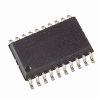
AT90PWM81-16SN Atmel, AT90PWM81-16SN Datasheet - Page 175

AT90PWM81-16SN
Manufacturer Part Number
AT90PWM81-16SN
Description
IC MCU AVR 8K FLASH ISP 20SOIC
Manufacturer
Atmel
Series
AVR® 90PWM Lightingr
Datasheet
1.AT90PWM81-16MN.pdf
(325 pages)
Specifications of AT90PWM81-16SN
Core Processor
AVR
Core Size
8-Bit
Speed
16MHz
Connectivity
SPI
Peripherals
Brown-out Detect/Reset, PWM, WDT
Number Of I /o
16
Program Memory Size
8KB (8K x 8)
Program Memory Type
FLASH
Eeprom Size
512 x 8
Ram Size
256 x 8
Voltage - Supply (vcc/vdd)
2.7 V ~ 5.5 V
Data Converters
A/D 8x10b; D/A 1x10b
Oscillator Type
Internal
Operating Temperature
-40°C ~ 105°C
Package / Case
20-SOIC (7.5mm Width)
Data Bus Width
8 bit
Data Ram Size
256 B
Interface Type
SPI
Maximum Clock Frequency
16 MHz
Number Of Timers
1
Maximum Operating Temperature
+ 105 C
Mounting Style
SMD/SMT
Minimum Operating Temperature
- 40 C
On-chip Adc
10 bit, 8 Channel
On-chip Dac
10 bit, 1 Channel
Height
2.35 mm
Length
13 mm
Supply Voltage (max)
5.5 V
Supply Voltage (min)
2.7 V
Width
7.6 mm
For Use With
ATSTK600-SOIC - STK600 SOCKET/ADAPTER FOR SOIC
Lead Free Status / RoHS Status
Lead free / RoHS Compliant
Available stocks
Company
Part Number
Manufacturer
Quantity
Price
Company:
Part Number:
AT90PWM81-16SN
Manufacturer:
Atmel
Quantity:
1 500
- Current page: 175 of 325
- Download datasheet (6Mb)
13.23.8
13.23.9
7734P–AVR–08/10
PSCR Input A Control Register – PFRC0A
PSCR Input B Control Register – PFRC0B
• Bit 5- PBFM01: Balance Flank Width Modulation, bit 1
Defines the Flank Width Modulation, together with PBFM00 bit.
Table 13-13.
1.
• Bit 4 – PAOC0B : PSCR Asynchronous Output Control B
When this bit is set, Fault input selected to block B can act directly to PSCOUT01 output. See
Section “PSCR Input Configuration”, page 159.
• Bit 3 – PAOC0A : PSCR Asynchronous Output Control A
When this bit is set, Fault input selected to block A can act directly to PSCOUT00 output. See
Section “PSCR Input Configuration”, page 159.
• Bit 2- PBFM00: Balance Flank Width Modulation, bit 0
Defines the Flank Width Modulation, together with PBFM01 bit
• Bit 1 – PCCYC0 : PSCR Complete Cycle
When this bit is set, the PSCR completes the entire waveform cycle before halt operation requested by
clearing PRUN0. This bit is not relevant in slave mode (PARUN0 = 1).
• Bit 0 – PRUN0 : PSCR Run
Writing this bit to one starts the PSCR.
When set, this bit prevails over PARUN0 bit.
Bit
Read/Write
Initial Value
Bit
Read/Write
Initial Value
PBFM01
0
0
1
1
Note: In one ramp mode, changing SA or SA+SB also affect On-Time ; see PSCr0 & PSCr1 Basic Wave-
forms in One Ramp mode
7
PCAE0A
R/W
0
7
PCAE0B
R/W
0
Flank Width Mode Selection
PBFM00
0
1
0
1
6
PISEL0A0 PELEV0A
R/W
0
6
PISEL0B0 PELEV0B
R/W
0
5
R/W
0
5
R/W
0
Description
Flank Width Modulation operates on RB (On-Time 1 only).
Flank Width Modulation operates on RB + RA (On-Time 0 and On-Time
1).
Flank Width Modulation operates on SB (Dead-Time 1 only)
Flank Width Modulation operates on SB +SA (Dead-Time 0 and Dead-
Time 1).
4
PFLTE0A
R/W
0
4
PFLTE0B
R/W
0
3
PRFM0A3 PRFM0A2 PRFM0A1 PRFM0A0 PFRC0A
R/W
0
3
PRFM0B3 PRFM0B2 PRFM0B1 PRFM0B0 PFRC0B
R/W
0
2
R/W
0
2
R/W
0
1
R/W
0
1
R/W
0
AT90PWM81
0
R/W
0
0
R/W
0
(1)
.
175
Related parts for AT90PWM81-16SN
Image
Part Number
Description
Manufacturer
Datasheet
Request
R

Part Number:
Description:
Manufacturer:
Atmel Corporation
Datasheet:

Part Number:
Description:
IC MCU AVR 8K FLASH ISP 32QFN
Manufacturer:
Atmel
Datasheet:

Part Number:
Description:
IC MCU AVR 8K FLASH ISP 32QFN
Manufacturer:
Atmel
Datasheet:

Part Number:
Description:
IC MCU AVR 8K FLASH ISP 20SOIC
Manufacturer:
Atmel
Datasheet:

Part Number:
Description:
8-bit Avr Microcontroller With 8k Bytes In- System Programmable Flash
Manufacturer:
ATMEL Corporation
Datasheet:

Part Number:
Description:
DEV KIT FOR AVR/AVR32
Manufacturer:
Atmel
Datasheet:

Part Number:
Description:
INTERVAL AND WIPE/WASH WIPER CONTROL IC WITH DELAY
Manufacturer:
ATMEL Corporation
Datasheet:

Part Number:
Description:
Low-Voltage Voice-Switched IC for Hands-Free Operation
Manufacturer:
ATMEL Corporation
Datasheet:

Part Number:
Description:
MONOLITHIC INTEGRATED FEATUREPHONE CIRCUIT
Manufacturer:
ATMEL Corporation
Datasheet:

Part Number:
Description:
AM-FM Receiver IC U4255BM-M
Manufacturer:
ATMEL Corporation
Datasheet:

Part Number:
Description:
Monolithic Integrated Feature Phone Circuit
Manufacturer:
ATMEL Corporation
Datasheet:

Part Number:
Description:
Multistandard Video-IF and Quasi Parallel Sound Processing
Manufacturer:
ATMEL Corporation
Datasheet:


