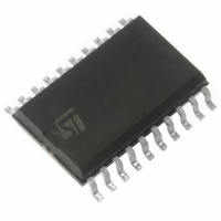
ST7FDALIF2M6TR STMicroelectronics, ST7FDALIF2M6TR Datasheet - Page 129

ST7FDALIF2M6TR
Manufacturer Part Number
ST7FDALIF2M6TR
Description
IC MCU 8BIT 8K FLASH 20-SOIC
Manufacturer
STMicroelectronics
Series
ST7r
Datasheet
1.ST7DALI-EVAL.pdf
(171 pages)
Specifications of ST7FDALIF2M6TR
Core Processor
ST7
Core Size
8-Bit
Speed
8MHz
Connectivity
DALI, SPI
Peripherals
LVD, POR, PWM, WDT
Number Of I /o
15
Program Memory Size
8KB (8K x 8)
Program Memory Type
FLASH
Eeprom Size
256 x 8
Ram Size
384 x 8
Voltage - Supply (vcc/vdd)
2.4 V ~ 5.5 V
Data Converters
A/D 7x10b
Oscillator Type
Internal
Operating Temperature
-40°C ~ 85°C
Package / Case
20-SOIC (7.5mm Width)
Processor Series
ST7DALI
Core
ST7
Data Bus Width
8 bit
Data Ram Size
384 B
Interface Type
DALI, SPI
Maximum Clock Frequency
8 MHz
Number Of Programmable I/os
15
Number Of Timers
3
Maximum Operating Temperature
+ 85 C
Mounting Style
SMD/SMT
Development Tools By Supplier
ST7FLITE-SK/RAIS, ST7DALI-EVAL, ST7MDT10-DVP3, ST7MDT10-EMU3, STX-RLINK
Minimum Operating Temperature
- 40 C
On-chip Adc
10 bit, 7 Channel / 13 bit, 7 Channel
Lead Free Status / RoHS Status
Lead free / RoHS Compliant
Available stocks
Company
Part Number
Manufacturer
Quantity
Price
Company:
Part Number:
ST7FDALIF2M6TR
Manufacturer:
NEC
Quantity:
670
ST7DALIF2
Table 63.
1.
2.
3.
4.
Table 64.
I
respected, the injection current must be limited externally to the I
while a negative injection is induced by V
corresponding V
Negative injection disturbs the analog performance of the device. In particular, it induces leakage currents throughout the
device including the analog inputs. To avoid undesirable effects on the analog functions, care must be taken:
- Analog input pins must have a negative injection less than 0.8 mA (assuming that the impedance of the analog voltage is
lower than the specified limits)
- Pure digital pins must have a negative injection less than 1.6mA. In addition, it is recommended to inject the current as
far as possible from the analog input pins.
No negative current injection allowed on PB0 and PB1 pins.
When several inputs are submitted to a current injection, the maximum ΣI
negative injected currents (instantaneous values). These results are based on characterization with ΣI
current injection on four I/O port pins of the device.
INJ(PIN)
I
INJ(PIN)
ΣI
Symbol
Symbol
INJ(PIN)
T
I
I
VDD
VSS
I
STG
T
IO
must never be exceeded. This is implicitly insured if V
J
(1) & (2)
Current characteristics
Thermal characteristics
2)
IN
maximum must always be respected
Total current into V
Total current out of V
Output current sunk by any standard I/O and
control pin
Output current sunk by any high sink I/O pin
Output current source by any I/Os and control
pin
Injected current on RESET pin
Injected current on OSC1 and OSC2 pins
Injected current on PB0 and PB1 pins
Injected current on any other pin
Total injected current (sum of all I/O and control
pins)
Storage temperature range
Maximum junction temperature (see
(4)
IN
<V
SS
DD
Ratings
. For true open-drain pads, there is no positive injection current, and the
Ratings
SS
power lines (source)
ground lines (sink)
IN
INJ(PIN)
maximum is respected. If V
(4)
Table 94 on page
value. A positive injection is induced by V
(3)
INJ(PIN)
is the absolute sum of the positive and
Maximum value
Electrical characteristics
-65 to +150
IN
160)
maximum cannot be
Value
± 20
150
- 25
± 5
± 5
± 5
75
20
40
+5
INJ(PIN)
maximum
IN
>V
129/171
Unit
Unit
mA
°C
DD


