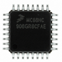
MCHC908GR8CFAE Freescale Semiconductor, MCHC908GR8CFAE Datasheet - Page 134

MCHC908GR8CFAE
Manufacturer Part Number
MCHC908GR8CFAE
Description
IC MCU FLSH 8BIT8MHZ 7.5K32-LQFP
Manufacturer
Freescale Semiconductor
Series
HC08r
Specifications of MCHC908GR8CFAE
Core Processor
HC08
Core Size
8-Bit
Speed
8MHz
Connectivity
SCI, SPI
Peripherals
LVD, POR, PWM
Number Of I /o
21
Program Memory Size
7.5KB (7.5K x 8)
Program Memory Type
FLASH
Ram Size
384 x 8
Voltage - Supply (vcc/vdd)
2.7 V ~ 5.5 V
Data Converters
A/D 6x8b
Oscillator Type
Internal
Operating Temperature
-40°C ~ 85°C
Package / Case
32-LQFP
Controller Family/series
HC08
No. Of I/o's
21
Ram Memory Size
384Byte
Cpu Speed
8MHz
No. Of Timers
2
Embedded Interface Type
I2C, SCI, SPI
Rohs Compliant
Yes
Processor Series
HC08G
Core
HC08
Data Bus Width
8 bit
Data Ram Size
384 B
Interface Type
SCI, SPI
Maximum Clock Frequency
8.2 MHz
Number Of Programmable I/os
21
Number Of Timers
3
Operating Supply Voltage
2.7 V to 5.5 V
Maximum Operating Temperature
+ 85 C
Mounting Style
SMD/SMT
Development Tools By Supplier
FSICEBASE, DEMO908GZ60E, M68CBL05CE, M68EML08GPGTE
Minimum Operating Temperature
- 40 C
On-chip Adc
8 bit, 6 Channel
Lead Free Status / RoHS Status
Lead free / RoHS Compliant
Eeprom Size
-
Lead Free Status / Rohs Status
Details
Available stocks
Company
Part Number
Manufacturer
Quantity
Price
Company:
Part Number:
MCHC908GR8CFAE
Manufacturer:
Freescale Semiconductor
Quantity:
10 000
Company:
Part Number:
MCHC908GR8CFAER
Manufacturer:
Freescale Semiconductor
Quantity:
10 000
- Current page: 134 of 292
- Download datasheet (4Mb)
Input/Output (I/O) Ports (PORTS)
When bit DDRDx is a 1, reading address $0003 reads the PTDx data latch. When bit DDRDx is a 0,
reading address $0003 reads the voltage level on the pin. The data latch can always be written,
regardless of the state of its data direction bit.
12.5.3 Port D Input Pullup Enable Register
The port D input pullup enable register (PTDPUE) contains a software configurable pullup device for each
of the eight port D pins. Each bit is individually configurable and requires that the data direction register,
DDRD, bit be configured as an input. Each pullup is automatically and dynamically disabled when a port
bit’s DDRD is configured for output mode.
PTDPUE7–PTDPUE0 — Port D Input Pullup Enable Bits
12.6 Port E
Port E is a 5-bit special-function port that shares two of its pins with the serial communications interface
(SCI) module and two of its pins with the internal clock generator (ICG).
134
1. X = Don’t care
2. I/O pin pulled up to V
3. Writing affects data register, but does not affect input.
4. Hi-Z = High imp[edance
PTDPUE
These writable bits are software programmable to enable pullup devices on an input port bit.
Bit
X
1
0
1 = Corresponding port D pin configured to have internal pullup
0 = Corresponding port D pin has internal pullup disconnected
Address:
DDRD
Reset:
Read:
Write:
Bit
0
0
1
MC68HC908GT16 • MC68HC908GT8 • MC68HC08GT16 Data Sheet, Rev. 5.0
Figure 12-16. Port D Input Pullup Enable Register (PTDPUE)
DD
PTDPUE7
$000F
Bit 7
by internal pullup device.
0
PTD
X
Bit
X
X
(1)
PTDPUE6
6
0
Input, Hi-Z
Input, V
Table 12-5. Port D Pin Functions
I/O Pin
Output
Mode
PTDPUE5
DD
(2)
(4)
5
0
Table 12-5
PTDPUE4
Accesses to DDRD
DDRD7–DDRD0
DDRD7–DDRD0
DDRD7–DDRD0
4
0
Read/Write
PTDPUE3
summarizes the operation of the port D pins.
3
0
PTDPUE2
2
0
PTD7–PTD0
Read
Pin
Pin
PTDPUE1
Accesses to PTD
1
0
Freescale Semiconductor
PTDPUE0
Bit 0
0
PTD7–PTD0
PTD7–PTD0
PTD7–PTD0
Write
(3)
(3)
Related parts for MCHC908GR8CFAE
Image
Part Number
Description
Manufacturer
Datasheet
Request
R
Part Number:
Description:
Manufacturer:
Freescale Semiconductor, Inc
Datasheet:
Part Number:
Description:
Manufacturer:
Freescale Semiconductor, Inc
Datasheet:
Part Number:
Description:
Manufacturer:
Freescale Semiconductor, Inc
Datasheet:
Part Number:
Description:
Manufacturer:
Freescale Semiconductor, Inc
Datasheet:
Part Number:
Description:
Manufacturer:
Freescale Semiconductor, Inc
Datasheet:
Part Number:
Description:
Manufacturer:
Freescale Semiconductor, Inc
Datasheet:
Part Number:
Description:
Manufacturer:
Freescale Semiconductor, Inc
Datasheet:
Part Number:
Description:
Manufacturer:
Freescale Semiconductor, Inc
Datasheet:
Part Number:
Description:
Manufacturer:
Freescale Semiconductor, Inc
Datasheet:
Part Number:
Description:
Manufacturer:
Freescale Semiconductor, Inc
Datasheet:
Part Number:
Description:
Manufacturer:
Freescale Semiconductor, Inc
Datasheet:
Part Number:
Description:
Manufacturer:
Freescale Semiconductor, Inc
Datasheet:
Part Number:
Description:
Manufacturer:
Freescale Semiconductor, Inc
Datasheet:
Part Number:
Description:
Manufacturer:
Freescale Semiconductor, Inc
Datasheet:
Part Number:
Description:
Manufacturer:
Freescale Semiconductor, Inc
Datasheet:


