MCHC908GR8CFAE Freescale Semiconductor, MCHC908GR8CFAE Datasheet - Page 92
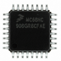
MCHC908GR8CFAE
Manufacturer Part Number
MCHC908GR8CFAE
Description
IC MCU FLSH 8BIT8MHZ 7.5K32-LQFP
Manufacturer
Freescale Semiconductor
Series
HC08r
Specifications of MCHC908GR8CFAE
Core Processor
HC08
Core Size
8-Bit
Speed
8MHz
Connectivity
SCI, SPI
Peripherals
LVD, POR, PWM
Number Of I /o
21
Program Memory Size
7.5KB (7.5K x 8)
Program Memory Type
FLASH
Ram Size
384 x 8
Voltage - Supply (vcc/vdd)
2.7 V ~ 5.5 V
Data Converters
A/D 6x8b
Oscillator Type
Internal
Operating Temperature
-40°C ~ 85°C
Package / Case
32-LQFP
Controller Family/series
HC08
No. Of I/o's
21
Ram Memory Size
384Byte
Cpu Speed
8MHz
No. Of Timers
2
Embedded Interface Type
I2C, SCI, SPI
Rohs Compliant
Yes
Processor Series
HC08G
Core
HC08
Data Bus Width
8 bit
Data Ram Size
384 B
Interface Type
SCI, SPI
Maximum Clock Frequency
8.2 MHz
Number Of Programmable I/os
21
Number Of Timers
3
Operating Supply Voltage
2.7 V to 5.5 V
Maximum Operating Temperature
+ 85 C
Mounting Style
SMD/SMT
Development Tools By Supplier
FSICEBASE, DEMO908GZ60E, M68CBL05CE, M68EML08GPGTE
Minimum Operating Temperature
- 40 C
On-chip Adc
8 bit, 6 Channel
Lead Free Status / RoHS Status
Lead free / RoHS Compliant
Eeprom Size
-
Lead Free Status / Rohs Status
Details
Available stocks
Company
Part Number
Manufacturer
Quantity
Price

Company:
Part Number:
MCHC908GR8CFAE
Manufacturer:
Freescale Semiconductor
Quantity:
10 000
Company:
Part Number:
MCHC908GR8CFAER
Manufacturer:
Freescale Semiconductor
Quantity:
10 000


Internal Clock Generator (ICG) Module)
7.4.4.4 Ring Oscillator Fine-Adjust Circuit
The ring oscillator fine-adjust circuit causes the ring oscillator to effectively operate at non-integer
numbers of stage delays by operating at two different points for a variable number of cycles specified by
the lower five DCO stage control bits (DSTG[4:0]). For example:
Adjusting the DSTG[0] bit has a 0.202 percent to 0.368 percent effect on the output clock period. This
corresponds to the minimum size correction made by the DLF, and the inherent, long-term quantization
error in the output frequency.
7.4.5 Switching Internal Clock Frequencies
The frequency of the internal clock (ICLK) may need to be changed for some applications. For example,
if the reset condition does not provide the correct frequency, or if the clock is slowed down for a low-power
mode (or sped up after a low-power mode), the frequency must be changed by programming the internal
clock multiplier factor (N). The frequency of ICLK is N times the frequency of IBASE, which is 307.2 kHz
±25 percent.
Before switching frequencies by changing the N value, the clock monitor must be disabled. This is
because when N is changed, the frequency of the low-frequency base clock (IBASE) will change
proportionally until the digital loop filter has corrected the error. Since the clock monitor uses IBASE, it
could erroneously detect an inactive clock. The clock monitor cannot be re-enabled until the internal clock
is stable again (ICGS is set).
The following flow is an example of how to change the clock frequency:
7.4.6 Nominal Frequency Settling Time
Because the clock period of the internal clock (ICLK) is dependent on the digital loop filter outputs (DDIV
and DSTG) which cannot change instantaneously, ICLK temporarily will operate at an incorrect clock
period when any operating condition changes. This happens whenever the part is reset, the ICG multiply
factor (N) is changed, the ICG trim factor (TRIM) is changed, or the internal clock is enabled after inactivity
(stop mode or disabled operation). The time that the ICLK takes to adjust to the correct period is known
as the settling time.
92
•
•
•
•
•
•
•
•
•
•
•
When DSTG[7:5] is %011, the ring oscillator nominally operates at 23 stage delays.
When DSTG[4:0] is %00000, the ring will always operate at 23 stage delays.
When DSTG[4:0] is %00001, the ring will operate at 25 stage delays for one of 32 cycles and at 23
stage delays for 31 of 32 cycles.
Likewise, when DSTG[4:0] is %11111, the ring operates at 25 stage delays for 31 of 32 cycles and
at 23 stage delays for one of 32 cycles.
When DSTG[7:5] is %111, similar results are achieved by including a variable divide-by-two, so the
ring operates at 31 stages for some cycles and at 17 stage delays, with a divide-by-two for an
effective 34 stage delays, for the remainder of the cycles.
Verify there is no clock monitor interrupt by reading the CMF bit.
Turn off the clock monitor.
If desired, switch to the external clock (see
Change the value of N.
Switch back to internal (see
Turn on the clock monitor (see
MC68HC908GT16 • MC68HC908GT8 • MC68HC08GT16 Data Sheet, Rev. 5.0
7.4.1 Switching Clock
7.4.2 Enabling the Clock
7.4.1 Switching Clock
Sources), if desired.
Monitor), if desired.
Sources).
Freescale Semiconductor
Related parts for MCHC908GR8CFAE
Image
Part Number
Description
Manufacturer
Datasheet
Request
R

Part Number:
Description:
Manufacturer:
Freescale Semiconductor, Inc
Datasheet:
Part Number:
Description:
Manufacturer:
Freescale Semiconductor, Inc
Datasheet:
Part Number:
Description:
Manufacturer:
Freescale Semiconductor, Inc
Datasheet:
Part Number:
Description:
Manufacturer:
Freescale Semiconductor, Inc
Datasheet:
Part Number:
Description:
Manufacturer:
Freescale Semiconductor, Inc
Datasheet:
Part Number:
Description:
Manufacturer:
Freescale Semiconductor, Inc
Datasheet:
Part Number:
Description:
Manufacturer:
Freescale Semiconductor, Inc
Datasheet:
Part Number:
Description:
Manufacturer:
Freescale Semiconductor, Inc
Datasheet:
Part Number:
Description:
Manufacturer:
Freescale Semiconductor, Inc
Datasheet:
Part Number:
Description:
Manufacturer:
Freescale Semiconductor, Inc
Datasheet:
Part Number:
Description:
Manufacturer:
Freescale Semiconductor, Inc
Datasheet:
Part Number:
Description:
Manufacturer:
Freescale Semiconductor, Inc
Datasheet:
Part Number:
Description:
Manufacturer:
Freescale Semiconductor, Inc
Datasheet:
Part Number:
Description:
Manufacturer:
Freescale Semiconductor, Inc
Datasheet:
Part Number:
Description:
Manufacturer:
Freescale Semiconductor, Inc
Datasheet: