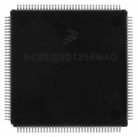
MC9S12XDT256MAG Freescale Semiconductor, MC9S12XDT256MAG Datasheet - Page 1276

MC9S12XDT256MAG
Manufacturer Part Number
MC9S12XDT256MAG
Description
IC MCU 256K FLASH 144-LQFP
Manufacturer
Freescale Semiconductor
Series
HCS12r
Datasheet
1.MC9S12XD64CAA.pdf
(1348 pages)
Specifications of MC9S12XDT256MAG
Core Processor
HCS12X
Core Size
16-Bit
Speed
80MHz
Connectivity
CAN, EBI/EMI, I²C, IrDA, LIN, SCI, SPI
Peripherals
LVD, POR, PWM, WDT
Number Of I /o
119
Program Memory Size
256KB (256K x 8)
Program Memory Type
FLASH
Eeprom Size
4K x 8
Ram Size
16K x 8
Voltage - Supply (vcc/vdd)
2.35 V ~ 5.5 V
Data Converters
A/D 24x10b
Oscillator Type
External
Operating Temperature
-40°C ~ 125°C
Package / Case
144-LQFP
Processor Series
S12XD
Core
HCS12
Data Bus Width
16 bit
Data Ram Size
16 KB
Interface Type
CAN/I2C/SCI/SPI
Maximum Clock Frequency
40 MHz
Number Of Programmable I/os
119
Number Of Timers
12
Operating Supply Voltage
0 V to 5.5 V
Maximum Operating Temperature
+ 125 C
Mounting Style
SMD/SMT
3rd Party Development Tools
EWHCS12
Development Tools By Supplier
EVB9S12XDP512E
Minimum Operating Temperature
- 40 C
On-chip Adc
2 (24-ch x 10-bit)
Lead Free Status / RoHS Status
Lead free / RoHS Compliant
Available stocks
Company
Part Number
Manufacturer
Quantity
Price
Company:
Part Number:
MC9S12XDT256MAG
Manufacturer:
Freescale Semiconductor
Quantity:
10 000
- Current page: 1276 of 1348
- Download datasheet (8Mb)
Appendix A Electrical Characteristics
In
In
1
1278
Num
0.5 t
Figure A-10
Table A-27
10
11
12
13
(CPOL = 0)
(CPOL = 1)
1
1
2
3
4
5
6
7
8
9
(Output)
bus
NOTE: Not defined
(Input)
(Input)
(Input)
(Input)
MISO
MOSI
SCK
SCK
added due to internal synchronization delay
SS
C
D
D
D
D
D
D
D
D
D
D
D
D
D
D
the timing characteristics for slave mode are listed.
SCK frequency
SCK period
Enable lead time
Enable lag time
Clock (SCK) high or low time
Data setup time (inputs)
Data hold time (inputs)
Slave access time (time to data active)
Slave MISO disable time
Data valid after SCK edge
Data valid after SS fall
Data hold time (outputs)
Rise and fall time inputs
Rise and fall time outputs
the timing diagram for slave mode with transmission format CPHA = 1 is depicted.
Note
See
7
2
Characteristic
Slave
4
5
Table A-27. SPI Slave Mode Timing Characteristics
9
MSB IN
1
Figure A-10. SPI Slave Timing (CPHA = 1)
MSB OUT
6
MC9S12XDP512 Data Sheet, Rev. 2.21
4
12
12
11
Bit 6 . . . 1
Bit 6 . . . 1
Symbol
t
t
t
wsck
t
f
t
t
lead
t
vsck
t
t
t
sck
sck
t
vss
t
lag
t
dis
ho
rfo
su
hi
rfi
a
Min
DC
20
—
—
—
—
—
—
4
4
4
4
8
8
13
13
Slave LSB OUT
3
LSB IN
Typ
—
—
—
—
—
—
—
—
—
—
—
—
—
—
29 + 0.5 t
29 + 0.5 t
Freescale Semiconductor
8
Max
1 4
20
22
—
—
—
—
—
—
8
8
bus
bus
1
1
Unit
f
t
t
t
t
bus
bus
bus
bus
bus
ns
ns
ns
ns
ns
ns
ns
ns
ns
Related parts for MC9S12XDT256MAG
Image
Part Number
Description
Manufacturer
Datasheet
Request
R

Part Number:
Description:
16-BIT MICROPROCESSOR FAMILY
Manufacturer:
FREESCALE [Freescale Semiconductor, Inc]
Datasheet:
Part Number:
Description:
Manufacturer:
Freescale Semiconductor, Inc
Datasheet:
Part Number:
Description:
Manufacturer:
Freescale Semiconductor, Inc
Datasheet:
Part Number:
Description:
Manufacturer:
Freescale Semiconductor, Inc
Datasheet:
Part Number:
Description:
Manufacturer:
Freescale Semiconductor, Inc
Datasheet:
Part Number:
Description:
Manufacturer:
Freescale Semiconductor, Inc
Datasheet:
Part Number:
Description:
Manufacturer:
Freescale Semiconductor, Inc
Datasheet:
Part Number:
Description:
Manufacturer:
Freescale Semiconductor, Inc
Datasheet:
Part Number:
Description:
Manufacturer:
Freescale Semiconductor, Inc
Datasheet:
Part Number:
Description:
Manufacturer:
Freescale Semiconductor, Inc
Datasheet:
Part Number:
Description:
Manufacturer:
Freescale Semiconductor, Inc
Datasheet:
Part Number:
Description:
Manufacturer:
Freescale Semiconductor, Inc
Datasheet:
Part Number:
Description:
Manufacturer:
Freescale Semiconductor, Inc
Datasheet:
Part Number:
Description:
Manufacturer:
Freescale Semiconductor, Inc
Datasheet:
Part Number:
Description:
Manufacturer:
Freescale Semiconductor, Inc
Datasheet:


