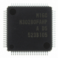
M30280FAHP#D5 Renesas Electronics America, M30280FAHP#D5 Datasheet - Page 201

M30280FAHP#D5
Manufacturer Part Number
M30280FAHP#D5
Description
IC M16C MCU FLASH 96K 80-LQFP
Manufacturer
Renesas Electronics America
Series
M16C™ M16C/Tiny/28r
Datasheet
1.M30280F6HPU9.pdf
(425 pages)
Specifications of M30280FAHP#D5
Core Processor
M16C/60
Core Size
16-Bit
Speed
20MHz
Connectivity
I²C, IEBus, SIO, UART/USART
Peripherals
DMA, POR, PWM, Voltage Detect, WDT
Number Of I /o
71
Program Memory Size
96KB (96K x 8)
Program Memory Type
FLASH
Ram Size
8K x 8
Voltage - Supply (vcc/vdd)
2.7 V ~ 5.5 V
Data Converters
A/D 24x10b
Oscillator Type
Internal
Operating Temperature
-20°C ~ 85°C
Package / Case
80-LQFP
For Use With
M30290T2-CPE - EMULATOR COMPACT M16C/26A/28/29M30290T2-CPE-HP - EMULATOR COMPACT FOR M16C/TINY
Lead Free Status / RoHS Status
Contains lead / RoHS non-compliant
Eeprom Size
-
Other names
M30280FAHP#D5A
Available stocks
Company
Part Number
Manufacturer
Quantity
Price
- Current page: 201 of 425
- Download datasheet (4Mb)
M
R
R
1
e
E
. v
6
J
0
C
2
9
2 /
0 .
B
8
0
0
14.1.1.1 Counter Measure for Communication Error Occurs
0
G
If a communication error occurs while transmitting or receiving in clock synchronous serial I/O mode,
follow the procedures below.
•Resetting the UiRB register (i=0 to 2)
•Resetting the UiTB register (i=0 to 2)
4
J
7
(1) Set the RE bit in the UiC1 register to “0” (reception disabled)
(2) Set the SMD2 to SMD0 bits in the UiMR register to “000
(3) Set the SMD2 to SMD0 bits in the UiMR register to “001
(4) Set the RE bit in the UiC1 register to “1” (reception enabled)
(1) Set the SMD2 to SMD0 bits in the UiMR register to “000
(2) Set the SMD2 to SMD0 bits in the UiMR register to “001
(3) “1” is written to TE bit in the UiC1 register (reception enabled), regardless to the TE bit.
a
o r
0 -
. n
u
2
p
3
0
, 1
0
(
M
2
1
0
0
6
7
C
2 /
, 8
page 179
M
1
6
C
2 /
f o
8
3
) B
8
5
2
2
2
2
” (Serial I/O disabled)
” (Clock synchronous serial I/O mode)
” (Serial I/O disabled)
” (Clock synchronous serial I/O mode)
14. Serial I/O
Related parts for M30280FAHP#D5
Image
Part Number
Description
Manufacturer
Datasheet
Request
R

Part Number:
Description:
KIT STARTER FOR M16C/29
Manufacturer:
Renesas Electronics America
Datasheet:

Part Number:
Description:
KIT STARTER FOR R8C/2D
Manufacturer:
Renesas Electronics America
Datasheet:

Part Number:
Description:
R0K33062P STARTER KIT
Manufacturer:
Renesas Electronics America
Datasheet:

Part Number:
Description:
KIT STARTER FOR R8C/23 E8A
Manufacturer:
Renesas Electronics America
Datasheet:

Part Number:
Description:
KIT STARTER FOR R8C/25
Manufacturer:
Renesas Electronics America
Datasheet:

Part Number:
Description:
KIT STARTER H8S2456 SHARPE DSPLY
Manufacturer:
Renesas Electronics America
Datasheet:

Part Number:
Description:
KIT STARTER FOR R8C38C
Manufacturer:
Renesas Electronics America
Datasheet:

Part Number:
Description:
KIT STARTER FOR R8C35C
Manufacturer:
Renesas Electronics America
Datasheet:

Part Number:
Description:
KIT STARTER FOR R8CL3AC+LCD APPS
Manufacturer:
Renesas Electronics America
Datasheet:

Part Number:
Description:
KIT STARTER FOR RX610
Manufacturer:
Renesas Electronics America
Datasheet:

Part Number:
Description:
KIT STARTER FOR R32C/118
Manufacturer:
Renesas Electronics America
Datasheet:

Part Number:
Description:
KIT DEV RSK-R8C/26-29
Manufacturer:
Renesas Electronics America
Datasheet:

Part Number:
Description:
KIT STARTER FOR SH7124
Manufacturer:
Renesas Electronics America
Datasheet:

Part Number:
Description:
KIT STARTER FOR H8SX/1622
Manufacturer:
Renesas Electronics America
Datasheet:

Part Number:
Description:
KIT DEV FOR SH7203
Manufacturer:
Renesas Electronics America
Datasheet:


