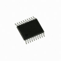
C8051F537-IT Silicon Laboratories Inc, C8051F537-IT Datasheet - Page 128

C8051F537-IT
Manufacturer Part Number
C8051F537-IT
Description
IC 8051 MCU 2K FLASH 20TSSOP
Manufacturer
Silicon Laboratories Inc
Series
C8051F53xr
Specifications of C8051F537-IT
Core Processor
8051
Core Size
8-Bit
Speed
25MHz
Connectivity
SPI, UART/USART
Peripherals
Brown-out Detect/Reset, POR, PWM, Temp Sensor, WDT
Number Of I /o
16
Program Memory Size
2KB (2K x 8)
Program Memory Type
FLASH
Ram Size
256 x 8
Voltage - Supply (vcc/vdd)
2 V ~ 5.25 V
Data Converters
A/D 16x12b
Oscillator Type
Internal
Operating Temperature
-40°C ~ 125°C
Package / Case
20-TSSOP
Lead Free Status / RoHS Status
Lead free / RoHS Compliant
Eeprom Size
-
Other names
336-1401
Available stocks
Company
Part Number
Manufacturer
Quantity
Price
Company:
Part Number:
C8051F537-IT
Manufacturer:
Silicon Labs
Quantity:
135
- Current page: 128 of 218
- Download datasheet (2Mb)
C8051F52x/F52xA/F53x/F53xA
In addition to performing general purpose I/O, P0 and P1 can generate a port match event if the logic lev-
els of the Port’s input pins match a software controlled value. A port match event is generated if
(P0 & P0MASK) does not equal (P0MATCH & P0MASK) or if (P1 & P1MASK) does not equal
(P1MATCH & P1MASK). This allows Software to be notified if a certain change or pattern occurs on P0 or
P1 input pins regardless of the XBRn settings. A port match event can cause an interrupt if EMAT (EIE2.1)
is set to 1 or cause the internal oscillator to awaken from SUSPEND mode. See Section “14.1.1. Internal
Oscillator Suspend Mode” on page 135 for more information.
SFR Definition 13.3. P0: Port0
SFR Definition 13.4. P0MDIN: Port0 Input Mode
128
Bits7–0: P0.[7:0]
Bits7–0: Analog Input Configuration Bits for P0.7–P0.0 (respectively).
P0.7
R/W
R/W
Bit7
Bit7
Write - Output appears on I/O pins per Crossbar Registers.
0: Logic Low Output.
1: Logic High Output (high impedance if corresponding P0MDOUT.n bit = 0).
Read - Always reads 0 if selected as analog input in register P0MDIN. Directly reads Port
pin when configured as digital input.
0: P0.n pin is logic low.
1: P0.n pin is logic high.
Port pins configured as analog inputs have their weak pullup, digital driver, and digital
receiver disabled.
0: Corresponding P0.n pin is configured as an analog input.
1: Corresponding P0.n pin is not configured as an analog input.
P0.6
R/W
R/W
Bit6
Bit6
P0.5
R/W
R/W
Bit5
Bit5
P0.4
R/W
R/W
Bit4
Bit4
Rev. 1.3
P0.3
R/W
R/W
Bit3
Bit3
P0.2
R/W
R/W
Bit2
Bit2
P0.1
R/W
R/W
Bit1
Bit1
SFR Address:
SFR Address:
P0.0
R/W
R/W
Bit0
Bit0
Addressable
Reset Value
Reset Value
11111111
11111111
0xF1
0x80
Bit
Related parts for C8051F537-IT
Image
Part Number
Description
Manufacturer
Datasheet
Request
R
Part Number:
Description:
SMD/C°/SINGLE-ENDED OUTPUT SILICON OSCILLATOR
Manufacturer:
Silicon Laboratories Inc
Part Number:
Description:
Manufacturer:
Silicon Laboratories Inc
Datasheet:
Part Number:
Description:
N/A N/A/SI4010 AES KEYFOB DEMO WITH LCD RX
Manufacturer:
Silicon Laboratories Inc
Datasheet:
Part Number:
Description:
N/A N/A/SI4010 SIMPLIFIED KEY FOB DEMO WITH LED RX
Manufacturer:
Silicon Laboratories Inc
Datasheet:
Part Number:
Description:
N/A/-40 TO 85 OC/EZLINK MODULE; F930/4432 HIGH BAND (REV E/B1)
Manufacturer:
Silicon Laboratories Inc
Part Number:
Description:
EZLink Module; F930/4432 Low Band (rev e/B1)
Manufacturer:
Silicon Laboratories Inc
Part Number:
Description:
I°/4460 10 DBM RADIO TEST CARD 434 MHZ
Manufacturer:
Silicon Laboratories Inc
Part Number:
Description:
I°/4461 14 DBM RADIO TEST CARD 868 MHZ
Manufacturer:
Silicon Laboratories Inc
Part Number:
Description:
I°/4463 20 DBM RFSWITCH RADIO TEST CARD 460 MHZ
Manufacturer:
Silicon Laboratories Inc
Part Number:
Description:
I°/4463 20 DBM RADIO TEST CARD 868 MHZ
Manufacturer:
Silicon Laboratories Inc
Part Number:
Description:
I°/4463 27 DBM RADIO TEST CARD 868 MHZ
Manufacturer:
Silicon Laboratories Inc
Part Number:
Description:
I°/4463 SKYWORKS 30 DBM RADIO TEST CARD 915 MHZ
Manufacturer:
Silicon Laboratories Inc
Part Number:
Description:
N/A N/A/-40 TO 85 OC/4463 RFMD 30 DBM RADIO TEST CARD 915 MHZ
Manufacturer:
Silicon Laboratories Inc
Part Number:
Description:
I°/4463 20 DBM RADIO TEST CARD 169 MHZ
Manufacturer:
Silicon Laboratories Inc


