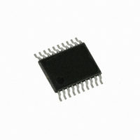
C8051F537-IT Silicon Laboratories Inc, C8051F537-IT Datasheet - Page 169

C8051F537-IT
Manufacturer Part Number
C8051F537-IT
Description
IC 8051 MCU 2K FLASH 20TSSOP
Manufacturer
Silicon Laboratories Inc
Series
C8051F53xr
Specifications of C8051F537-IT
Core Processor
8051
Core Size
8-Bit
Speed
25MHz
Connectivity
SPI, UART/USART
Peripherals
Brown-out Detect/Reset, POR, PWM, Temp Sensor, WDT
Number Of I /o
16
Program Memory Size
2KB (2K x 8)
Program Memory Type
FLASH
Ram Size
256 x 8
Voltage - Supply (vcc/vdd)
2 V ~ 5.25 V
Data Converters
A/D 16x12b
Oscillator Type
Internal
Operating Temperature
-40°C ~ 125°C
Package / Case
20-TSSOP
Lead Free Status / RoHS Status
Lead free / RoHS Compliant
Eeprom Size
-
Other names
336-1401
Available stocks
Company
Part Number
Manufacturer
Quantity
Price
Company:
Part Number:
C8051F537-IT
Manufacturer:
Silicon Labs
Quantity:
135
- Current page: 169 of 218
- Download datasheet (2Mb)
17.4. LIN Slave Mode Operation
When the device is configured for slave mode operation, it must wait for a command from a master node.
Access from the firmware to data buffer and ID registers of the LIN peripheral is only possible when a data
request is pending (DTREQ bit (LIN0ST.4) is 1) and also when the LIN bus is not active (ACTIVE bit
(LIN0ST.7) is set to 0).
The LIN peripheral in slave mode detects the header of the message frame sent by the LIN master. If slave
synchronization is enabled (autobaud), the slave synchronizes its internal bit time to the master bit time.
The LIN peripheral configured for slave mode will generated an interrupt in one of three situations:
1. After the reception of the IDENTIFIER FIELD.
2. When an error is detected.
3. When the message transfer is completed.
The application should perform the following steps when an interrupt is detected:
1. Check the status of the DTREQ bit (LIN0ST.4). This bit is set when the IDENTIFIER FIELD has been
2. If DTREQ (LIN0ST.4) is set, read the identifier from LIN0ID and process it. If DTREQ (LIN0ST.4) is not
3. Set the TXRX bit (LIN0CTRL.5) to 1 if the current frame is a transmit operation for the slave and set to
4. Load the data length into LIN0SIZE.
5. For a slave transmit operation, load the data to transmit into the data buffer.
6. Set the DTACK bit (LIN0CTRL.4). Continue to step 10.
7. If DTREQ (LIN0ST.4) is not set, check the DONE bit (LIN0ST.0). The transmission was successful if the
8. If the transmission was successful and the current frame was a receive operation for the slave, load the
9. If the transmission was not successful, check LIN0ERR to determine the nature of the error. Further
10.Set the RSTINT (LIN0CTRL.3) and RSTERR bits (LIN0CTRL.2) to reset the interrupt request and the
In addition to these steps, the application should be aware of the following:
1. If the current frame is a transmit operation for the slave, steps 1 through 5 must be completed during
2. If the current frame is a receive operation for the slave, steps 1 through 5 have to be finished until the
3. The LIN module does not directly support LIN Version 1.3 Extended Frames. If the application detects
4. Changing the configuration of the checksum during a transaction will cause the interface to reset and
received.
set, continue to step 7.
0 if the current frame is a receive operation for the slave.
DONE bit is set.
received data bytes from the data buffer.
error handling has to be done by the application.
error flags.
the IN-FRAME RESPONSE SPACE. If it is not completed in time, a timeout will be detected by the
master.
reception of the first byte after the IDENTIFIER FIELD. Otherwise, the internal receive buffer of the LIN
peripheral will be overwritten and a timeout error will be detected in the LIN peripheral.
an unknown identifier (e.g. extended identifier), it has to write a 1 to the STOP bit (LIN0CTRL.7) instead
of setting the DTACK (LIN0CTRL.4) bit. At that time, steps 2 through 5 can then be skipped. In this
situation, the LIN peripheral stops the processing of the LIN communication until the next SYNC
BREAK is received.
the transaction to be lost. To prevent this, the checksum should not be configured while a transaction is
C8051F52x/F52xA/F53x/F53xA
Rev. 1.3
169
Related parts for C8051F537-IT
Image
Part Number
Description
Manufacturer
Datasheet
Request
R
Part Number:
Description:
SMD/C°/SINGLE-ENDED OUTPUT SILICON OSCILLATOR
Manufacturer:
Silicon Laboratories Inc
Part Number:
Description:
Manufacturer:
Silicon Laboratories Inc
Datasheet:
Part Number:
Description:
N/A N/A/SI4010 AES KEYFOB DEMO WITH LCD RX
Manufacturer:
Silicon Laboratories Inc
Datasheet:
Part Number:
Description:
N/A N/A/SI4010 SIMPLIFIED KEY FOB DEMO WITH LED RX
Manufacturer:
Silicon Laboratories Inc
Datasheet:
Part Number:
Description:
N/A/-40 TO 85 OC/EZLINK MODULE; F930/4432 HIGH BAND (REV E/B1)
Manufacturer:
Silicon Laboratories Inc
Part Number:
Description:
EZLink Module; F930/4432 Low Band (rev e/B1)
Manufacturer:
Silicon Laboratories Inc
Part Number:
Description:
I°/4460 10 DBM RADIO TEST CARD 434 MHZ
Manufacturer:
Silicon Laboratories Inc
Part Number:
Description:
I°/4461 14 DBM RADIO TEST CARD 868 MHZ
Manufacturer:
Silicon Laboratories Inc
Part Number:
Description:
I°/4463 20 DBM RFSWITCH RADIO TEST CARD 460 MHZ
Manufacturer:
Silicon Laboratories Inc
Part Number:
Description:
I°/4463 20 DBM RADIO TEST CARD 868 MHZ
Manufacturer:
Silicon Laboratories Inc
Part Number:
Description:
I°/4463 27 DBM RADIO TEST CARD 868 MHZ
Manufacturer:
Silicon Laboratories Inc
Part Number:
Description:
I°/4463 SKYWORKS 30 DBM RADIO TEST CARD 915 MHZ
Manufacturer:
Silicon Laboratories Inc
Part Number:
Description:
N/A N/A/-40 TO 85 OC/4463 RFMD 30 DBM RADIO TEST CARD 915 MHZ
Manufacturer:
Silicon Laboratories Inc
Part Number:
Description:
I°/4463 20 DBM RADIO TEST CARD 169 MHZ
Manufacturer:
Silicon Laboratories Inc


