STEVAL-IPE010V1 STMicroelectronics, STEVAL-IPE010V1 Datasheet - Page 55
STEVAL-IPE010V1
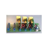
Manufacturer Part Number
STEVAL-IPE010V1
Description
KIT DEMO ENERGY METER STPMC1/S1
Manufacturer
STMicroelectronics
Type
Other Power Managementr
Specifications of STEVAL-IPE010V1
Main Purpose
Power Management, Energy/Power Meter
Embedded
No
Utilized Ic / Part
STPMC1, STPMS1
Maximum Operating Temperature
+ 85 C
Product
Power Management Development Tools
Lead Free Status / RoHS Status
Lead free / RoHS Compliant
Secondary Attributes
-
Primary Attributes
-
Lead Free Status / Rohs Status
Lead free / RoHS Compliant
For Use With/related Products
STPMC1, STPMS1
Other names
497-10754


STPMC1
Table 31.
0000000
0000001
0000010
0000011
0000100
0000101
0000110
0000111
Binary
7-BIT
Address
Each configuration bit can be written sending a byte command to STPMC1 through its SPI
interface. See paragraph
A system signal WE (see paragraph
some OTP bit. There is also a special high voltage input pad VOTP, which delivers the power
level necessary for permanent write to OTP cell.
The STPMC1 can work either using the data stored in the OTP cells or the data from the
shadow latches. This is done through the RD system signal (see paragraph
set, the CFG bits originates from corresponding OTP shadow latches otherwise, if RD is
cleared, the CFG bits originates from corresponding OTP antifuses. In this way it is possible
to test temporary configurators and calibrators before writing permanently on the device, for
example during meter production tests.
The very first CFG bit, called TSTD, disables any further OTP writing. After TSTD bit has
been set, the only commands accepted are the mode signal precharge (see paragraph
9.20
disabled and shadow latches cannot be used as source of configuration data anymore.
The following table represents a collection and function of all configuration bits in the device.
For multibit configurations the most significant bit address is bold .
Configuration bits map
DEC
0
1
2
3
4
5
6
7
) and the remote reset request (see paragraph
Name
FUND
TSTD
MDIV
HSA
TCS
FRS
APL
N. of
bits
1
1
1
2
1
1
9.21
IMPORTANT: The decimal value indicated in this column represents
Test mode and OTP write disable:
- TSTD=0: enable test modes and system signals,
- TSTD=1: normal operation and no more writes to OTP or test modes
Selection of measurement clock option:
- MDIV=0: f
- MDIV=1: f
High speed analog clock selection:
- HSA=0: f
- HSA=1: f
Application type selection:
- APL=0: peripheral MOP, MON=ZCR, WatchDOG, LED=pulses (X),
- APL=1: peripheral MOP, MON=stepper(P), LED=pulses (X),
- APL=2: standalone MOP, MON=stepper(P), LED=pulses(P),
- APL=3: standalone, MOP,MON=stepper(P) LED=pulses (P/64)
SCLNLC=no-load, SDATD=tamper indicator, SYN=neg act power
Type of current sensor selection:
- TCS=0: Rogowski coil,
- TCS=1: Current transformer (CT)
Nominal base frequency:
- FRS=0: 50Hz
- FRS=1: 60Hz
Fundamental active and reactive energy:
- FUND=0: full bandwidth active energy controls the stepper;
full bandwidth reactive energy computation.
- FUND=1: fundamental active energy controls the stepper;
fundamental reactive energy computation
SCLNLC=no-load SDATD=tamper detected, SYN=neg act power
Doc ID 15728 Rev 4
for details on SPI operation.
the value of the configuration bits with MSB in bold.
CLK
CLK
MCLK
MCLK
9.20
= f
= f
= f
= f
) is used in order to do the permanent write of
XTAL1
XTAL1
XTAL1
XTAL1
/4,
/2
* 2,
9.21.1
Description
), this implies that the test mode is
Theory of operation
9.20
). If RD is
55/77
Related parts for STEVAL-IPE010V1
Image
Part Number
Description
Manufacturer
Datasheet
Request
R

Part Number:
Description:
BOARD DEMO TFT DISPLAY STR91
Manufacturer:
STMicroelectronics
Datasheet:

Part Number:
Description:
BOARD EVAL FOR MEMS SENSORS
Manufacturer:
STMicroelectronics
Datasheet:

Part Number:
Description:
KIT DEV STARTER ST10F276Z5
Manufacturer:
STMicroelectronics
Datasheet:

Part Number:
Description:
BOARD EVAL HDMI $ VIDEO SWITCH
Manufacturer:
STMicroelectronics
Datasheet:

Part Number:
Description:
BOARD DEMO ACCELEROMETER DIL24
Manufacturer:
STMicroelectronics
Datasheet:

Part Number:
Description:
BOARD STLM75/STDS75/ST72F651
Manufacturer:
STMicroelectronics
Datasheet:

Part Number:
Description:
EVAL BOARD 3AXIS MEMS ACCELLRMTR
Manufacturer:
STMicroelectronics
Datasheet:

Part Number:
Description:
BOARD EVAL 8BIT MICRO + TDE1708
Manufacturer:
STMicroelectronics
Datasheet:

Part Number:
Description:
EVAL BOARD A/D TS4657
Manufacturer:
STMicroelectronics
Datasheet:

Part Number:
Description:
BOARD ADAPTER 20DIP LIS3LV02DL
Manufacturer:
STMicroelectronics
Datasheet:
Part Number:
Description:
STMicroelectronics [RIPPLE-CARRY BINARY COUNTER/DIVIDERS]
Manufacturer:
STMicroelectronics
Datasheet:
Part Number:
Description:
STMicroelectronics [LIQUID-CRYSTAL DISPLAY DRIVERS]
Manufacturer:
STMicroelectronics
Datasheet:
Part Number:
Description:
BOARD EVAL FOR MEMS SENSORS
Manufacturer:
STMicroelectronics
Datasheet: