STEVAL-IPE010V1 STMicroelectronics, STEVAL-IPE010V1 Datasheet - Page 65
STEVAL-IPE010V1
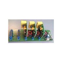
Manufacturer Part Number
STEVAL-IPE010V1
Description
KIT DEMO ENERGY METER STPMC1/S1
Manufacturer
STMicroelectronics
Type
Other Power Managementr
Specifications of STEVAL-IPE010V1
Main Purpose
Power Management, Energy/Power Meter
Embedded
No
Utilized Ic / Part
STPMC1, STPMS1
Maximum Operating Temperature
+ 85 C
Product
Power Management Development Tools
Lead Free Status / RoHS Status
Lead free / RoHS Compliant
Secondary Attributes
-
Primary Attributes
-
Lead Free Status / Rohs Status
Lead free / RoHS Compliant
For Use With/related Products
STPMC1, STPMS1
Other names
497-10754


STPMC1
9.21.4
9.21.5
t
t
t
t
t
t
t
t
Interfacing the standard 3-wire SPI with STPMC1 SPI
Due to the fact that a 2-wire SPI is implemented in the STPMC1, it is clear that sending any
command from a standard 3-wire SPI would require 3-wire to 2-wire interface, which should
produce a proper signal on SDATD from host signals SDI, SDO and SYN. A single gate 3-
state buffer could be omitted by an emulation of SPI just to send some command. On a
microcontroller this would be done by the following steps:
1.
2.
3.
4.
5.
6.
7.
8.
9.
10. enable the SPI module
In case of precharge command (0xFF), emulation above is not necessary. Due to the pull up
device on the SDATD pin of the STPMC1 the processor needs to perform the following
steps:
1.
2.
3.
4.
5.
6.
Permanent writing of the CFG bits
In order to make a permanent set of some CFG bits, the following procedure should
be conducted:
3
4
3
3
5
6
8
9
: data value is placed in SDA
: SDA value is stable and shifted into the device
: end of SPI writing
: SPI enters idle state
−>
−>
−>
−>
disable the SPI module
set SDI pin which is connected to SDATD to be output
activate SYN first and then SCS
apply new bit value to SDI and activate SCL
deactivate SCL
repeat the last two steps seven times to complete one byte transfer
repeat the last three steps for any remaining byte transfer
set SDI pin to be input
deactivate SCS and the SYN
activate SYN first in order to latch the result;
after at least 1 s activate SCS
write one byte to the transmitter of SPI (this produces 8 pulses on SCL with SDI = 1)
deactivate SYN
optionally read the data records (the sequence of reading is altered
deactivate SCS
t
t
t
t
5
5
6
7
: 1 bit data value
: 6 bits address of the destination latch
: 1 bit EXE command
(> 10 µs): writing clock period
Doc ID 15728 Rev 4
Theory of operation
65/77
Related parts for STEVAL-IPE010V1
Image
Part Number
Description
Manufacturer
Datasheet
Request
R

Part Number:
Description:
BOARD DEMO TFT DISPLAY STR91
Manufacturer:
STMicroelectronics
Datasheet:

Part Number:
Description:
BOARD EVAL FOR MEMS SENSORS
Manufacturer:
STMicroelectronics
Datasheet:

Part Number:
Description:
KIT DEV STARTER ST10F276Z5
Manufacturer:
STMicroelectronics
Datasheet:

Part Number:
Description:
BOARD EVAL HDMI $ VIDEO SWITCH
Manufacturer:
STMicroelectronics
Datasheet:

Part Number:
Description:
BOARD DEMO ACCELEROMETER DIL24
Manufacturer:
STMicroelectronics
Datasheet:

Part Number:
Description:
BOARD STLM75/STDS75/ST72F651
Manufacturer:
STMicroelectronics
Datasheet:

Part Number:
Description:
EVAL BOARD 3AXIS MEMS ACCELLRMTR
Manufacturer:
STMicroelectronics
Datasheet:

Part Number:
Description:
BOARD EVAL 8BIT MICRO + TDE1708
Manufacturer:
STMicroelectronics
Datasheet:

Part Number:
Description:
EVAL BOARD A/D TS4657
Manufacturer:
STMicroelectronics
Datasheet:

Part Number:
Description:
BOARD ADAPTER 20DIP LIS3LV02DL
Manufacturer:
STMicroelectronics
Datasheet:
Part Number:
Description:
STMicroelectronics [RIPPLE-CARRY BINARY COUNTER/DIVIDERS]
Manufacturer:
STMicroelectronics
Datasheet:
Part Number:
Description:
STMicroelectronics [LIQUID-CRYSTAL DISPLAY DRIVERS]
Manufacturer:
STMicroelectronics
Datasheet:
Part Number:
Description:
BOARD EVAL FOR MEMS SENSORS
Manufacturer:
STMicroelectronics
Datasheet: